
Datasheet
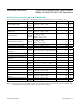

Voltages Referenced to GND
V
CC
........................................................................................+7V
FAULT, DE/RE, RE, DE, DE, DI, TXD ...... -0.3V to (V
CC
+ 0.3V)
A, B (Note 1) .......................................................................±60V
RO ............................................................ -0.3V to (V
CC
+ 0.3V)
Short-Circuit Duration (RO, A, B) ..............................Continuous
Continuous Power Dissipation (T
A
= +70°C)
SO (derate 5.9mW/°C above +70°C) ..........................471mW
PDIP (derate 9.09mW/°C above +70°C) .....................727mW
Operating Temperature Ranges
MAX344_EE_ _ .............................................. -40°C to +85°C
MAX344_EA_ _ ............................................ -40°C to +125°C
Storage Temperature Range ............................ -65°C to +150°C
Junction Temperature ...................................................... +150°C
Lead Temperature (soldering, 10s) .................................+300°C
Soldering Temperature (reflow) ....................................... +260°C
(V
CC
= +4.75V to +5.25V, T
A
= T
MIN
to T
MAX
, unless otherwise noted. Typical values are at V
CC
= +5V and T
A
= +25°C.)
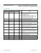
PARAMETER SYMBOL CONDITIONS MIN TYP MAX UNITS
DRIVER
Differential Driver Output V
OD
Figure 1, R
L
= 100Ω 2 V
CC
V
Figure 1, R
L
= 54Ω 1.5 V
CC
Change in Magnitude of
Differential Output Voltage
∆V
OD
Figure 1, R
L
= 100Ω or 54Ω (Note 2) 0.2 V
Driver Common-Mode
Output Voltage
V
OC
Figure 1, R
L
= 100Ω or 54Ω V
CC
/ 2 3 V
Change in Magnitude of
Common-Mode Voltage
∆V
OC
Figure 1, R
L
= 100Ω or 54Ω (Note 2) 0.2 V
DRIVER LOGIC
Driver Input High Voltage V
DIH
2 V
Driver Input Low Voltage V
DIL
0.8 V
Driver Input Current I
DIN
±2 µA
Driver Short-Circuit Output Current
(Note 3)
I
OSD
0V ≤ V
OUT
≤ +12V +350
mA
-7V ≤ V
OUT
≤ V
CC
-350
Driver Short-Circuit Foldback
Output Current
I
OSDF
(V
CC
- 1V) ≤ V
OUT
≤ +12V (Note 3) +25
mA
-7V ≤ V
OUT
≤ +1V (Note 3) -25
RECEIVER
Input Current I
A,B
A, B
V
CC
= GND, V
A, B
= 12V 250
µA
V
A, B
= -7V -150
V
A, B
= ±60V ±6 mA
Receiver Differential Threshold
Voltage
V
TH
-7V ≤ V
CM
≤ +12V -200 -50 mV
Receiver Input Hysteresis ∆V
TH
25 mV
www.maximintegrated.com
Maxim Integrated
│
2
MAX3440E–MAX3444E ±15kV ESD-Protected, ±60V Fault-Protected,
10Mbps, Fail-Safe RS-485/J1708 Transceivers
DC Electrical Characteristics
Stresses beyond those listed under “Absolute Maximum Ratings” may cause permanent damage to the device. These are stress ratings only, and functional operation of the device at these
or any other conditions beyond those indicated in the operational sections of the specifications is not implied. Exposure to absolute maximum rating conditions for extended periods may affect
device reliability.
Note 1: A, B must be terminated with 54Ω or 100Ω to guarantee ±60V fault protection.
Absolute Maximum Ratings