
Datasheet


MAX3362
3.3V, High-Speed, RS-485/RS-422 Transceiver in
SOT Package
_______________________________________________________________________________________ 7
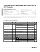
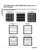
Pin Description
PIN NAME DESCRIPTION
1RO
Receiver Output. RO is high if the receiver input differential (A-B) ≥ 200mV and the receiver is enabled
(RE is low). RO is low if the receiver input differential (A-B) ≤ -200mV and the receiver is enabled.
2 RE
Receiver Output Enable. Driving RE low enables RO. RO is high impedance when RE is high. Drive RE
high and DE low (disable both receiver and driver outputs) to enter low-power shutdown mode.
3DE
Driver Output Enable. Driving DE high enables driver outputs. These outputs are high impedance
when DE is low. Drive RE high and DE low (disable both receiver and driver outputs) to enter low-
power shutdown mode.
4DI
D r i ver Inp ut. D r i vi ng D I l ow for ces the noni nver ti ng outp ut l ow and i nver ti ng outp ut hi g h, w hen the d r i ver i s
enab l ed ( D E i s hi g h) . D r i vi ng D I hi g h for ces the noni nver ti ng outp ut hi g h and i nver ti ng outp ut l ow .
5 GND Ground
6 A Noninverting Receiver Input and Noninverting Driver Output
7 B Inverting Receiver Input and Inverting Driver Output
8V
CC
Supply Voltage. V
CC
= 3.3V ±5%. Bypass V
CC
to GND with a 0.1µF capacitor.
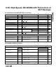
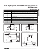
OUT
V
CC
R
L
C
L
D
C
L
= 50pF
R
L
= 54Ω
Figure 2. Driver Timing Test Circuit
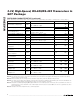
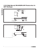
0
V
CC
/2
V
CC
B
A
t
PDLH
(A+B)/2
A - B
10%
90%
t
PDHL
t
ri
t
fi
t
ri
= 5ns
t
fi
= 5ns
t
DF
t
DR
DI
Figure 3. Driver Propagation Delay
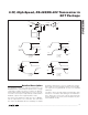
V
OD
V
CC
R
L
/2
R
L
/2
V
OC
D
Figure 1. Driver DC Test Load
IN
OUT
t
PDSL
, t
PDZL
t
PDLZ
0.25V
V
OL
0
V
CC
/2
V
OM
= (V
OL
+ V
CC
) /2
V
CC
V
CC
V
CC
R
L
= 500Ω
C
L
= 50pF
GENERATOR
50Ω
0 or 3V
OUT
S1
D
Figure 4. Driver Enable and Disable Times (t
PDSL
, t
PDZL
, t
PDLS
,
t
PDLZ
)