
Datasheet


MAX3362
3.3V, High-Speed, RS-485/RS-422 Transceiver in
SOT Package
2 _______________________________________________________________________________________
ABSOLUTE MAXIMUM RATINGS
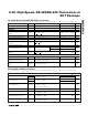
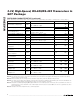
DC ELECTRICAL CHARACTERISTICS
(V
CC
= +3.3V ±5%, T
A
= T
MIN
to T
MAX
, unless otherwise noted. Typical values are at V
CC
= +3.3V and T
A
= +25°C.) (Notes 1, 2)
Stresses beyond those listed under “Absolute Maximum Ratings” may cause permanent damage to the device. These are stress ratings only, and functional
operation of the device at these or any other conditions beyond those indicated in the operational sections of the specifications is not implied. Exposure to
absolute maximum rating conditions for extended periods may affect device reliability.
All voltages with respect to GND.
V
CC
, RE, DE, DI ......................................................-0.3V to +6V
Receiver Input Voltages, Driver Output
Voltages (A, B) .......................................................-8V to +13V
Receiver Input Current, Driver Output
Current (A, B) .................................................................250mA
|V
A
- V
B
|..................................................................................+8V
Receiver Output Voltage (RO)....................-0.3V to (V
CC
+ 0.3V)
Continuous Power Dissipation (T
A
= +70°C)
8-Pin SOT (derate 9.7mW/°C above +70°C) ............... 777mW
Operating Temperature Range
MAX3362E__ .................................................. -40°C to +85°C
MAX3362A__ ................................................ -40°C to +125°C
Storage Temperature Range .............................-65°C to +150°C
Junction Temperature......................................................+150°C
Lead Temperature (soldering, 10s) .................................+300°C
PARAMETER SYMBOL CONDITIONS MIN TYP MAX UNITS
DRIVER
Figure 1, R
L
= 100Ω (RS-422)
(extended temperature range)
2.0
Figure 1, R
L
= 100Ω
(automotive temperature range)
1.5
Differential Driver Output V
OD
Figure 1, R
L
= 54Ω (RS-485)
(extended temperature range)
1.5
V
Change in Magnitude of
Differential Output Voltage
ΔV
OD
Figure 1, R
L
= 54Ω or 100Ω
(Note 3)
0.2 V
Driver Common-Mode Output
Voltage
V
OC
Figure 1, R
L
= 54Ω or 100Ω 3V
Change In Magnitude of
Common-Mode Voltage
ΔV
OC
Figure 1, R
L
= 54Ω or 100Ω
(Note 3)
0.2 V
Input High Voltage V
IH
DE, DI, RE 2.0 V
Input Low Voltage V
IL
DE, DI, RE 0.8 V
Input Hysteresis V
HYS
DE, DI, RE 50 mV
Input Current (DE, DI, RE)I
IN
0 < V
IN
< 5V ±1µA
0 < V
OUT
< 12V (Note 4) +250
Driver Short-Circuit Output
Current
I
OSD
-7V < V
OUT
< V
CC
(Note 4) -250
mA
(V
CC
- 1V) < V
OUT
< 12V (Note 4) +25
Driver Short-Circuit Foldback
Output Current
I
OSDF
-7V < V
OUT
< 1V (Note 4) -25
mA