
Datasheet
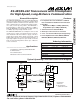


MAX3291/MAX3292
RS-485/RS-422 Transceivers with Preemphasis
for High-Speed, Long-Distance Communication
2 _______________________________________________________________________________________
ABSOLUTE MAXIMUM RATINGS
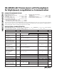
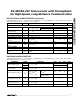
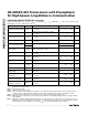
DC ELECTRICAL CHARACTERISTICS
(Typical Operating Circuit, V
CC
= +5V ±5%, R
PSET
= 0 (MAX3292), V
CC
= V
CCD
(MAX3292), T
A
= T
MIN
to T
MAX
, unless otherwise
noted. Typical values are at V
CC
= +5V and T
A
= +25°C.) (Note 1)
Stresses beyond those listed under “Absolute Maximum Ratings” may cause permanent damage to the device. These are stress ratings only, and functional
operation of the device at these or any other conditions beyond those indicated in the operational sections of the specifications is not implied. Exposure to
absolute maximum rating conditions for extended periods may affect device reliability.
Supply Voltage (V
CC
, V
CCD
) .................................................+6V
Control Input Voltage (
RE, DE, PEE,
PSET, DI).................................................-0.3V to (V
CC
+ 0.3V)
Driver Output Voltage (Y, Z)................................-7.5V to +12.5V
Receiver Input Voltage (A, B)..............................-7.5V to +12.5V
Receiver Output Voltage (RO)....................-0.3V to (V
CC
+ 0.3V)
Continuous Power Dissipation (T
A
= +70°C)
14-Pin SO (derate 8.7mW/°C above +70°C).................695mW
14-Pin Plastic DIP (derate 10.0mW/°C above +70°C) ..800mW
Operating Temperature Ranges
MAX329_C_ D......................................................0°C to +70°C
MAX329_E_ D...................................................-40°C to +85°C
Storage Temperature Range.............................-65°C to +160°C
Lead Temperature (soldering, 10sec).............................+300°C
R = 27Ω
DE = GND,
V
CC
= GND or 5.25V
V
PSET
= V
CC
DE, DI, RE
DE, DI, RE, PEE
DE, DI, RE
CONDITIONS
V2.4V
ODP
Differential Driver Output with
Preemphasis
µA
-25
I
O
Output Leakage (Y and Z)
25
µA70 110I
PSET
PSET Input Current (MAX3292)
V
2.4
V
IH
Input High Voltage
V0.8V
IL
Input Low Voltage
µA±2I
IN
Input Current
µA-15 -30 -45I
PEE
PEE Input Current (MAX3291)
UNITSMIN TYP MAXSYMBOLPARAMETER
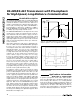
Figure 1, R = 27Ω (Note 3) V1.65 2.0 2.35DPER
Differential Driver
Preemphasis Ratio
Figure 1, R = 27Ω (Note 4) V0.2
∆V
OD
,
∆V
ODP
Change in Magnitude of
Differential Output Voltage
(Normal and Preemphasis)
Figure 1, R = 27Ω VV
CC
/ 2 3V
OC
Driver Common-Mode Output
Voltage (Normal and
Preemphasis)
Figure 1, R = 27Ω (Note 5) V0.3∆V
OC
Change in Magnitude of
Common-Mode Voltage
(Normal and Preemphasis)
Figure 1, R = 27Ω mV50∆V
NP
Change in Magnitude of
Common-Mode Output
Voltage (Normal to
Preemphasis)
-7V ≤ V
OUT
≤ +12V (Note 6) mA±30 ±250I
OSD
Driver Short-Circuit Output
Current
V
Y
= V
Z
= +12V
V
Y
= V
Z
= -7V
R = 27Ω
Figure 1
No load (Note 2)
V
5.25
V
OD
1.5 5.0
Differential Driver Output
PEE 3.75
DRIVER