
Datasheet


MAX199
Multi-Range (±4V, ±2V, +4V, +2V),
+5V Supply, 12-Bit DAS with 8+4 Bus Interface
_______________________________________________________________________________________ 7
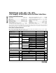
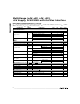
______________________________________________________________Pin Description
Digital GroundDGND28
+5V Supply. Bypass with 0.1µF capacitor to AGND.V
DD
27
INT goes low when conversion is complete and output data is ready.INT24
Bandgap Voltage-Reference Output / External Adjust Pin. Bypass with a 0.01µF capacitor to AGND.
Connect to V
DD
when using an external reference at the REF pin.
REFADJ25
Reference Buffer Output / ADC Reference Input. In internal reference mode, the reference buffer provides a
4.096V nominal output, externally adjustable at REFADJ. In external reference mode, disable the internal
buffer by pulling REFADJ to V
DD
.
REF26
Three-State Digital I/O. D2 output (HBEN = low), D10 output (HBEN = high).D2/D1012
Three-State Digital I/O. D1 output (HBEN = low), D9 output (HBEN = high).D1/D913
Three-State Digital I/O. D0 output (HBEN = low), D8 output (HBEN = high). D0 = LSB.D0/D814
Analog GroundAGND15
Analog Input ChannelsCH0–CH716–23
Used to multiplex the 12-bit conversion result. When high, the 4 MSBs are multiplexed on the data bus;
when low, the 8 LSBs are available on the bus.
HBEN5
Shutdown. Puts the device into full power-down (FULLPD) mode when pulled low.SHDN6
Three-State Digital I/OD7–D47–10
Three-State Digital I/O. D3 output (HBEN = low), D11 output (HBEN = high).D3/D1111
When CS is low, a falling edge on RD will enable a read operation on the data bus.RD4
When CS is low, in the internal acquisition mode, a rising edge on WRlatches in configuration data and starts an
acquisition plus a conversion cycle. When CSis low, in the external acquisition mode, the first rising edge on
WR starts an acquisition and a second rising edge on WRends acquisition and starts a conversion cycle.
WR3
PIN
Chip Select, active low.CS2
Clock Input. In external clock mode, drive CLK with a TTL/CMOS compatible clock. In internal clock mode,
place a capacitor (C
CLK
) from this pin to ground to set the internal clock frequency; f
CLK
= 1.56MHz typical
with C
CLK
= 100pF.
CLK1
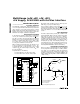
FUNCTIONNAME
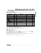
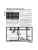
100k
510k
24k
REFADJ
+5V
0.01µF
MAX199
Figure 1. Reference-Adjust Circuit
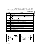
3k
3k
D
OUT
D
OUT
+5V
a) High-Z to V
OH
and V
OL
to V
OH
b) High-Z to V
OL
and V
OH
to V
OL
C
LOAD
C
LOAD
Figure 2. Load Circuits for Enable Time