
Datasheet


MAX199
Multi-Range (±4V, ±2V, +4V, +2V),
+5V Supply, 12-Bit DAS with 8+4 Bus Interface
_______________________________________________________________________________________ 3
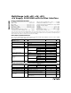
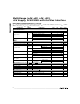
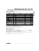
ELECTRICAL CHARACTERISTICS (continued)
(V
DD
= 5V ±5%; unipolar/bipolar range; external reference mode, V
REF
= 4.096V; 4.7µF at REF pin; external clock, f
CLK
= 2.0MHz
with 50% duty cycle; T
A
= T
MIN
to T
MAX
, unless otherwise noted.)
f
CLK
= 2.0MHz
MAX199_C
T
A
= +25°C
(Note 5)
Unipolar (see Table 2)
CONDITIONS
mA30Output Short-Circuit Current
ppm/°C
±15
REF Output Tempco
(
Contact Maxim Applications
for guaranteed temperature
drift specifications
)
V4.076 4.096 4.116V
REF
REF Output Voltage
pF40Input Capacitance
µs3Track/Hold Acquisition Time
0V
REF/2
V
0V
REF
Input Voltage Range
1.25
-3dB rolloff
2.5
UNITSMIN TYP MAXSYMBOLPARAMETER
MHz
5
Small-Signal Bandwidth
2.5
Bipolar
-600 10
Unipolar range
-1200 10±V
REF
range
±V
REF/2
range
Bipolar
0.1 10
Unipolar
10
MΩ40
Input Dynamic Resistance
Bipolar (see Table 2)
-V
REF/2
V
REF/2
-V
REF
V
REF
0mA to 0.5mA output current (Note 6) 7.5
V2.465 2.500 2.535REFADJ Output Voltage
µF4.7Capacitive Bypass at REF
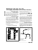
With recommended circuit (Figure 1) %±1.5REFADJ Adjustment Range
V/V1.6384Buffer Voltage Gain
V2.4 4.18Input Voltage Range
µA
400
Input Current V
REF
= 4.18V
1
VV
DD
- 50mV
REFADJ Threshold for
Buffer Disable
Normal, or STANDBY power-down mode kΩ10
Input Resistance
FULL power-down mode 5 MΩ
±V
REF
range
±V
REF/2
range
0V to V
REF
range
0V to V
REF/2
range
Normal, or STANDBY
power-down mode
FULL power-down
mode
TC V
REF
µAInput Current
MAX199_M ±40
MAX199_E ±30
kΩ
0mA to 0.1mA output current (Note 6)
mV
0.8
Load Regulation
ANALOG INPUT
INTERNAL REFERENCE
REFERENCE INPUT (Buffer disabled, reference input applied to REF pin)