
Datasheet
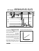


Transfer Function
Output data coding for the MAX199 is binary in unipolar
mode with 1LSB = (FS / 4096) and twos-complement
binary in bipolar mode with 1LSB = [(2 x
|
FS
|
) / 4096].
Code transitions occur halfway between successive-
integer LSB values. Figures 10 and 11 show the
input/output (I/O) transfer functions for unipolar and
bipolar operations, respectively.
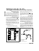
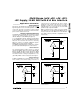
Layout, Grounding, and Bypassing
Careful printed circuit board layout is essential for best
system performance. For best performance, use a
ground plane. To reduce crosstalk and noise injection,
keep analog and digital signals separate. Digital
ground lines can run between digital signal lines to
minimize interference. Connect analog grounds and
DGND in a star configuration to AGND. For noise-free
operation, ensure the ground return from AGND to the
supply ground is low impedance and as short as possi-
ble. Connect the logic grounds directly to the supply
ground. Bypass V
DD
with 0.1µF and 4.7µF capacitors
to AGND to minimize high- and low-frequency fluctua-
tions. If the supply is excessively noisy, connect a 5Ω
resistor between the supply and V
DD
, as shown in
Figure 12.
MAX199
Multi-Range (±4V, ±2V, +4V, +2V),
+5V Supply, 12-Bit DAS with 8+4 Bus Interface
______________________________________________________________________________________ 15
_Ordering Information (continued)
28 Narrow Ceramic SB**-55°C to +125°CMAX199BMYI
28 Narrow Ceramic SB**-55°C to +125°CMAX199AMYI
28 SSOP-40°C to +85°CMAX199BEAI
28 SSOP-40°C to +85°CMAX199AEAI
28 Wide SO-40°C to +85°CMAX199BEWI
28 Wide SO
28 Narrow Plastic DIP
28 Narrow Plastic DIP-40°C to +85°C
-40°C to +85°C
-40°C to +85°CMAX199AEWI
MAX199BENI
MAX199AENI
PIN-PACKAGETEMP. RANGEPART
V
DD
GND
DGND
DGNDAGND
+5V
+5V
SUPPLY
R* = 5Ω
DIGITAL
CIRCUITRY
4.7µF
0.1µF
MAX199
**
* OPTIONAL
** CONNECT AGND AND DGND WITH A GROUND PLANE OR A SHORT TRACE
Figure 12. Power-Supply Grounding Connection
TRANSISTOR COUNT: 2956
SUBSTRATE CONNECTED TO GND
___________________Chip Topography
CH5
CH6
CH7
INT
REFADJ
0.231"
(5.870mm)
0.144"
(3.659mm)
D2
CH0
CH1D0
D1
AGND
CH4
CH3
CH2
V
CC
V
DD
REFDGND
CLKWR
CS
RD
HBEN
SHDN
D7
D6
D5
D4
D3
**
Contact factory for availability and processing to MIL-STD-883.