
Datasheet


How to Read a Conversion
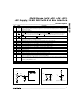
A standard interrupt signal, INT, is provided to allow the
device to flag the µP when the conversion has ended
and a valid result is available. INT goes low when the
conversion is complete and the output data is ready
(Figures 5 and 6). It returns high on the first read cycle
or if a new control byte is written.
Clock Modes
The MAX199 operates with either an internal or an
external clock. Control bits (D6, D7) select either inter-
nal or external clock mode. Once the desired clock
mode is selected, changing these bits to program
power-down will not affect the clock mode. In each
mode, internal or external acquisition can be used. At
power-up, the MAX199 defaults to external clock mode.
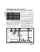
Internal Clock Mode
Select internal clock mode to free the µP from the
burden of running the SAR conversion clock. To select
this mode, write the control byte with D7 = 0 and D6 = 1.
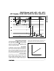
A 100pF capacitor between the CLK pin and ground
sets this frequency to 1.56MHz nominal. Figure 7
shows a linear relationship between the internal clock
period and the value of the external capacitor used.
MAX199
Multi-Range (±4V, ±2V, +4V, +2V),
+5V Supply, 12-Bit DAS with 8+4 Bus Interface
______________________________________________________________________________________ 11
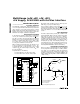
t
CS
t
CSWS
t
WR
t
ACQI
t
CONV
t
DH
t
DS
t
INT1
t
D0
t
D01
t
TR
t
CSHW
t
CSRS
t
CSRH
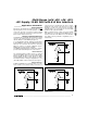
ACQMOD = "1"
CS
WR
D7–D0
INT
RD
HBEN
DOUT
ACQMOD = "0"
HIGH / LOW
BYTE VALID
HIGH-Z HIGH-Z
HIGH / LOW
BYTE VALID
CONTROL
BYTE
CONTROL
BYTE
Figure 6. Conversion Timing Using External Acquisition Mode
2000
0
0 50 250 350
500
CLOCK PIN CAPACITANCE (pF)
INTERNAL CLOCK PERIOD (ns)
100 150 200 300
1500
1000
Figure 7. Internal Clock Period vs. Clock Pin Capacitance