
Datasheet


MAX197
Multi-Range (±10V, ±5V, +10V, +5V),
Single +5V, 12-Bit DAS with 8+4 Bus Interface
8 _______________________________________________________________________________________
_______________Detailed Description
Converter Operation
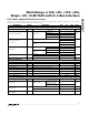
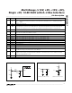
The MAX197, a multi-range, fault-tolerant ADC, uses
successive approximation and internal input track/hold
(T/H) circuitry to convert an analog signal to a 12-bit
digital output. The parallel-output format provides easy
interface to microprocessors (µPs). Figure 3 shows the
MAX197 in its simplest operational configuration.
Analog-Input Track/Hold
In the internal acquisition control mode (control bit D5
set to 0), the T/H enters its tracking mode on WR’s ris-
ing edge, and enters its hold mode when the internally
timed (6 clock cycles) acquisition interval ends. A low
impedance input source, which settles in less than
1.5µs, is required to maintain conversion accuracy at
the maximum conversion rate.
In the external acquisition control mode (D5 = 1), the
T/H enters its tracking mode on the first WR rising edge
and enters its hold mode when it detects the second WR
rising edge with D5 = 0. See the External Acquisition
section.
Input Bandwidth
The ADC’s input tracking circuitry has a 5MHz small-
signal bandwidth. When using the internal acquisition
mode with an external clock frequency of 2MHz, a
100ksps throughput rate can be achieved. It is possible
to digitize high-speed transient events and measure
periodic signals with bandwidths exceeding the ADC’s
sampling rate by using undersampling techniques. To
avoid high-frequency signals being aliased into the fre-
quency band of interest, anti-alias filtering is recom-
mended (MAX274/MAX275 continuous-time filters).
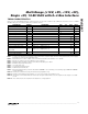
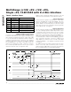
Input Range and Protection
Figure 4 shows the equivalent input circuit. With V
REF
=
4.096V, the MAX197 can be programmed for input
ranges of ±10V, ±5V, 0V to 10V, or 0V to 5V by setting the
appropriate control bits (D3, D4) in the control byte (see
Tables 2 and 3). The full-scale input voltage depends on
the voltage at REF (Table 1). When an external reference
is applied at REFADJ, the voltage at REF is given by V
REF
= 1.6384 x V
REFADJ
(2.4V < V
REF
< 4.18V).
DGND
V
DD
REF
REFADJ
INT
CH7
CH6
CH5
CH4
CH3
CH2
CH1
CH0
AGND
28
27
26
4.7µF
0.1µF
+5V
+4.096V
OUTPUT STATUS
25
24
23
22
21
20
19
18
17
16
1
2
µP
CONTROL
INPUTS
3
4
5
6
CLK
CS
WR
RD
HBEN
SHDN
D7
D6
D5
D4
D3/D11
D2/D10
D1/D9
D0/D8
100pF
µP DATA BUS
15
7
8
9
10
11
12
13
14
ANALOG
INPUTS
MAX197
Figure 3. Operational Diagram
5.12k
Ω
8.67kΩ
12.5k
Ω
CH_
S1
S2
S3
S4
BIPOLAR
UNIPOLAR
VOLTAGE
REFERENCE
T/H
OUT
HOLDTRACK
TRACKHOLD
OFF
ON
C
HOLD
S1 = BIPOLAR/UNIPOLAR SWITCH
S2 = INPUT MUX SWITCH
S3, S4 = T/H SWITCH
Figure 4. Equivalent Input Circuit
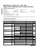
RANGE (V)
ZERO SCALE
(V) -FULL SCALE +FULL SCALE
0 to 5 0 — V
REF
x 1.2207
0 to 10 0 — V
REF
x 2.4414
±5 — -V
REF
x 1.2207 V
REF
x 1.2207
±10 — -V
REF
x 2.4414 V
REF
x 2.4414
Table 1. Full Scale and Zero Scale