
Datasheet


Layout, Grounding, and Bypassing
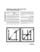
Careful printed circuit board layout is essential for best
system performance. For best performance, use a
ground plane. To reduce crosstalk and noise injection,
keep analog and digital signals separate. Digital
ground lines can run between digital signal lines to
minimize interference. Connect analog grounds and
DGND in a star configuration to AGND. For noise-free
operation, ensure the ground return from AGND to the
supply ground is low impedance and as short as possi-
ble. Connect the logic grounds directly to the supply
ground. Bypass V
DD
with 0.1µF and 4.7µF capacitors
to AGND to minimize high- and low-frequency fluctua-
tions. If the supply is excessively noisy, connect a 5Ω
resistor between the supply and V
DD
, as shown in
Figure 12.
MAX196/MAX198
Multirange, Single +5V, 12-Bit DAS
with 12-Bit Bus Interface
______________________________________________________________________________________ 15
V
DD
GND
DGND
DGNDAGND
+5V
+5V
SUPPLY
R* = 5Ω
DIGITAL
CIRCUITRY
4.7µF
0.1µF
MAX196
MAX198
**
* OPTIONAL
** CONNECT AGND AND DGND WITH A GROUND PLANE OR A SHORT TRACE
Figure 12. Power-Supply Grounding Connection
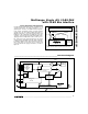
_________________________________________________________Functional Diagram
T/H
THREE-STATE, BIDIRECTIONAL
I/O INTERFACE
12
10k
12
8
CHARGE REDISTRIBUTION
12-BIT DAC
CLOCK
SIGNAL
CONDITIONING
BLOCK
&
OVERVOLTAGE
TOLERANT
MUX
CONTROL LOGIC
&
LATCHES
REF REFADJ
+2.5V
REFERENCE
D0–D11
12-BIT DATA BUS
CH5
CH4
CH3
CH2
CH1
CH0
CLK
CS
WR
RD
INT
V
DD
AGND
DGND
MAX196
MAX198
A
V
=
1.638
COMP
SUCCESSIVE-
APPROXIMATION
REGISTER