
Datasheet


MAX195
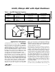
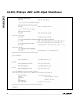
An OR gate is used to synchronize the “start” signal to
the asynchronous CLK, as described in the
External
Clock
section. As with Mode 1, the QSPI processor must
run CLK during calibration and either count CLK cycles
or, as is done here, monitor EOC to determine when cal-
ibration is complete. Also, EOC is polled by the µP to
determine when a conversion result is available. When
EOC goes low, data is clocked out at the highest QSPI
data rate (4.19Mbps). After the data is transferred, a
new conversion can be initiated whenever desired.
The timing specification for SCLK-to-DOUT valid (t
SD
)
imposes some constraints on the serial interface. At
SCLK rates up to 2.5Mbps, data is clocked out of the
MAX195 by a falling edge of SCLK and may be
clocked into the µP by the next rising edge (CPOL = 0,
CPHA = 0). For data rates greater than 2.5Mbps (or for
lower rates, if desired) it is necessary to clock data out
of the MAX195 on SCLK’s falling edge and to clock it
into the µP on SCLK’s next falling edge (CPOL = 0,
CPHA = 1). Also, your processor hold time must not
exceed t
SD
minimum (20ns). As with CLK in mode 1,
maximum SCLK rates may not be possible with some
interface specifications that are subsets of SPI.
Supplies, Layout, Grounding
and Bypassing
For best system performance, use printed circuit
boards with separate analog and digital ground planes.
Wire-wrap boards are not recommended. The two
ground planes should be tied together at the low-
impedance power-supply source and at the MAX195
(Figure 22.) If the analog and digital supplies come
from the same source, isolate the digital supply from
the analog supply with a low-value resistor (10Ω).
Constraints on sequencing the four power supplies are
as follows.
• Apply VDDA before VDDD.
• Apply VSSA before VSSD.
• Apply AIN and REF after VDDA and VSSA are present.
• The power supplies should settle within the
MAX195’s power-on delay (minimum 500ns) or you
should recalibrate the converter (pulse RESET low)
before use.
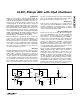
16-Bit, 85ksps ADC with 10µA Shutdown
18 ______________________________________________________________________________________
CS
CLK
START
588ns
239ns
CONVERSION TIME
4.19MHz
1.3µs 9.4µs 17µs* 5.1µs
4µs
EOC
SCLK
DOUT
B15 B3 B2B13B14 B1 B0
* INTERRUPT LATENCY OF THE PROCESSOR
Figure 20. Timing Diagram for Circuit of Figure 19 (Mode 2)