
Datasheet


If clocking data in on the falling edge (CPOL = 0,
CPHA = 1), the maximum CLK rate is given by:
Do not exceed the maximum CLK frequency given in
the
Electrical Characteristics
table. To clock data in on
the falling edge, your processor hold time must not
exceed t
CD
minimum (100ns).
While QSPI can provide the required 20 CLK cycles as
two continuous 10-bit transfers, SPI is limited to 8-bit
transfers. This means that with SPI, a conversion must
consist of three 8-bit transfers. Ensure that the pauses
between 8-bit operations at your selected clock rate
are short enough to maintain a 20ms or shorter conver-
sion time, or the leakage of the capacitive DAC may
cause errors.
Complete source code for the Motorola 68HC16 and
the MAX195 evaluation kit (EV kit) using this mode is
available with the MAX195 EV kit.
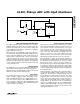
Mode 2 (Asynchronous Data Transfer)
This mode uses a conversion clock (CLK) and a serial
clock (SCLK). The serial data is clocked out between
conversions, which reduces the maximum throughput
for high CLK rates, but may be more convenient for
some applications. Figure 19 is a block diagram with a
QSPI processor (Motorola 68HC16) connected to the
MAX195. Figure 20 shows the associated timing dia-
gram. Figure 21 gives an assembly language listing for
this arrangement.
f =
1
t + t
CLK(max)
CD SD
MAX195
16-Bit, 85ksps ADC with 10µA Shutdown
______________________________________________________________________________________ 17
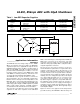
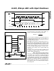
EOC
CLK
t
CD
t
DV
DATA LATCHED:
t
DH
CS, CONV
DOUT
B15 FROM PREVIOUS
CONVERSION
B15 B15B2B14 B1 B0
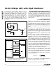
MAX195
QSPI
GPT
BP/UP/SHDN
SCLK
EOC
DOUT
RESET
CONV
1.7MHz
CLKIC3
CS
OC3
SCK
IC1
MISO
OC2
START
PCS0
1.3µs
74HC32
Figure 19. MAX195 Connection to QSPI Processor Clocking
Data Out with SCLK Between Conversions
Figure 18. Timing Diagram for Circuit of Figure 17 (Mode 1)