
Datasheet


MAX195
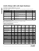
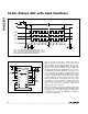
Data is clocked out on SCLK’s falling edge. Clock
data in on SCLK’s rising edge or, for clock speeds
above 2.5MHz, on the following falling edge to meet
the maximum SCLK-to-DOUT timing specification
(Figure 7). The maximum SCLK speed is 5MHz. See
the
Operating Modes and SPI/QSPI Interfaces
section
for additional information. When the conversion clock
is near its maximum (1.7MHz), reading the data after
each conversion (during the acquisition time) results
in lower throughput (about 70ksps max) than reading
the data during conversions, because it takes longer
than the minimum input acquisition time (four cycles
at 1.7MHz) to clock 16 data bits at 5Mbps. After the
data has been clocked in, leave some time (about
1µs) for any coupled noise on AIN to settle before
beginning the next conversion.
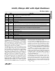
Whichever method is chosen for reading the data, con-
versions can be individually initiated by bringing CONV
low, or they can occur continuously by connecting EOC
to CONV. Figure 8 shows the MAX195 in its simplest
operational configuration.
16-Bit, 85ksps ADC with 10µA Shutdown
10 ______________________________________________________________________________________
EOC
CS
SCLK
(CASE 1)
SCLK
(CASE 2)
CASE 1: SCLK IDLES LOW, DATA LATCHED ON RISING EDGE (CPOL = 0, CPHA = 0)
CASE 2: SCLK IDLES LOW, DATA LATCHED ON FALLING EDGE (CPOL = 0, CPHA = 1)
CASE 3: SCLK IDLES HIGH, DATA LATCHED ON FALLING EDGE (CPOL = 1, CPHA = 0)
NOTE: ARROWS ON SCLK TRANSITIONS INDICATE LATCHING EDGE
DOUT
SCLK
(CASE 3)
t
CONV
t
DH
t
SD
t
DV
MSB LSB
B15
B14 B13 B12 B3 B2 B1
B0
B11
t
CSS
t
CSH
MAX195
10µF
BP/UP/
SHDN
CLK
SCLK
VDDD
DOUT
DGND
REFERENCE
(0V TO VDDA)
ANALOG
INPUT
-5V
EOC
CS
VDDA
VSSA
AGND
AIN
CONVERSION
CLOCK
+5V
REF
VSSD
RESET
CONV
0.1µF
10µF
0.1µF
1
2
3
4
5
6
7
8
16
15
14
13
12
11
10
9
Figure 7. Output Data Format, Reading Data Between Conversions (Mode 2)
Figure 8. MAX195 in the Simplest Operating Configuration