
Datasheet


MAX1778/MAX1880–MAX1885
Quad-Output TFT LCD DC/DC
Converters with Buffer
30
Maxim Integrated
Capacitor Selection and Regulator Stability
Capacitors are required at the input and output of the
MAX1778/MAX1881/MAX1883/MAX1884 for stable
operation over the full temperature range and with load
currents up to 40mA. Connect a 1µF input bypass
capacitor (C
SUPL
) between SUPL and ground to lower
the source impedance of the input supply. Connect a
ceramic capacitor between LDOOUT and ground,
using the following equation to determine the lowest
value required for stable operation:
For example, with a 5V linear regulator output voltage
and a maximum 40mA load, use at least 4µF of output
capacitance. Applications that experience high-current
load pulses may require more output capacitance.
The ESR of the linear regulator’s output capacitor
(C
LDOOUT
) affects stability and output noise. Use output
capacitors with an ESR of 0.1Ω or less to ensure stability
and optimum transient response. Surface-mount ceram-
ic capacitors are good for this purpose. Place C
SUPL
and C
LDOOUT
as close as possible to the linear regula-
tor to minimize the impact of PCB trace inductance.
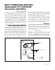
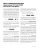
External Pass Transistor
For applications where the linear regulator currents
exceed 40mA or where the power dissipation in the IC
needs to be reduced, an external npn transistor can be
used. In this case, the internal LDO only provides the
necessary base drive while the external npn transistor
supports the load, so most of the power dissipation occurs
across the external transistor’s collector and emitter.
Selection of the external npn transistor is based on
three factors: the package’s power dissipation, the cur-
rent gain (β), and the collector-to-emitter saturation volt-
age (V
CE(SAT)
). First, the maximum power dissipation
should not exceed the transistor’s package rating:
Once the appropriate package type is selected,
consider the npn transistor’s current gain. Since the
internal LDO cannot source more than 40mA (min), the
transistor’s current gain must be high enough at the
lowest collector-to-emitter voltage to support the
maximum output load:
For stable operation, place a capacitor (C
LDOOUT
) and
a minimum load resistor (R5) at the output of the inter-
nal linear regulator (the base of the external transistor)
to set the dominant pole:
Since the LDO cannot sink current, a minimum pull-
down resistor (R5) is required at the base of the npn
transistor to sink leakage currents and improve the
high-to-low load-transient response. Under no-load
conditions, leakage currents from the internal pass
transistor supply the output capacitor (C
LDOOUT
), even
when the transistor is off. As the leakage currents
increase over temperature, charge can build up on
C
LDOOUT
, making the linear regulator’s output rise
above its set point. Therefore, R5 must sink at least
100µA to guarantee proper regulation. Additionally, the
minimum load current provided by R5 improves the
high-to-low load transients by lowering the impedance
seen by C
LDOOUT
after the transient occurs. Therefore,
if large load transients are expected, select R5 so that
the minimum load current is 10% of the transistor’s
maximum base current:
Alternatively, output capacitance placed on the external
linear regulator’s output (the emitter) adds a second pole
that could destabilize the regulator. A capacitive-divider
from the transistor’s base to the feedback input (C2 and
C3, Figure 7) circumvents this second pole by adding a
pole-zero pair. Furthermore, to minimize excessive over-
shoot, the capacitive-divider’s ratio must be the same as
the resistive-divider’s ratio. Once the output capacitor is
selected, using the following equations to determine the
required capacitive-divider values:
CC
CR
R
C
CC
R
RR
V
V
LDO
REF
LDO
23
100
1
4
3
2
23
4
34
+≥ +
⎛
⎝
⎜
⎞
⎠
⎟
+
=
+
=
R
VV
I
VV
I
LDO
LDOOUT MIN
LDO MI
N
LOAD MAX
5
07
01
07
.
.
( .)
() ( )
=
+
=
+
⎡
⎣
⎢
⎢
β
Cms
V
x
VV
R
I
LDOOUT
LDO
LDO
LOAD MAX
MIN
.
.
()
≥
⎛
⎝
⎜
⎞
⎠
⎟
+
+
⎛
⎝
⎜
⎞
⎠
⎟
05
1
07
5 β
β
MIN
LOAD MAX
ImA
mA
()
≥
-40
40
PV V xI
COLLECTOR LDO LOAD MAX
( )
()
=−
CmsX
I
V
LDOOUT
LDOOUT MAX
LDOOUT
.
()
≥
⎛
⎝
⎜
⎜
⎞
⎠
⎟
⎟
05