
Datasheet


MAX1778/MAX1880–MAX1885
Quad-Output TFT LCD DC/DC
Converters with Buffer
29
Maxim Integrated
at higher output currents (see the
Typical Operating
Characteristics
). So the maximum efficiency can be
approximated by:
for the positive charge pump, and:
for the negative charge pump, where V
SUPD
is the
positive charge pump’s diode supply (Figure 4).
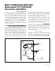
Output-Voltage Selection
Adjust the positive output voltage by connecting a volt-
age-divider from the output (V
POS
) to FBP to GND (see
the
Typical Operating Circuit
). Adjust the negative
output voltage by connecting a voltage-divider from the
output (V
NEG
) to FBN to REF. Select R4 and R6 in the
50kΩ to 100kΩ range. Higher resistor values improve
efficiency at low output current but increase output-
voltage error due to the feedback input bias current. For
the negative charge pump, higher resistor values also
reduce the load on the reference, which should not
exceed 50µA for greatest accuracy (including current
through the FLTSET resistors) to guarantee that V
REF
remains in regulation (see the
Electrical Characteristics
).
Calculate the remaining resistors with the following
equations:
R3 = R4 [(V
POS
/V
REF
) - 1]
R5 = R6 |V
NEG
/V
R
EF
|
where V
REF
= 1.25V. V
POS
can range from V
SUPP
to
40V, and V
NEG
can range from 0V to -40V.
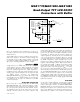
Flying Capacitor
Increasing the flying capacitor (CX) value increases the
output current capability. Above a certain point,
increasing the capacitance has a negligible effect
because the output current capability becomes domi-
nated by the internal switch resistance and the diode
impedance. The flying capacitor’s voltage rating must
exceed the following:
for the positive charge pump, and:
for the negative charge pump, where N is the stage
number in which the flying capacitor appears, and
V
SUPD
is the positive charge pump’s diode supply
(Figure 4). For example, the two-stage positive charge
pump in the typical application circuit (Figure 1) where
V
SUPP
= V
SUPD
= 8V contains two flying capacitors.
The flying capacitor in the first stage (C4) requires a
voltage rating over 12V. The flying capacitor in the
second stage (C6) requires a voltage rating over 24V.
Charge-Pump Output Capacitor
Increasing the output capacitance or decreasing the
ESR reduces the output ripple voltage and the peak-to-
peak transient voltage. With ceramic capacitors, the
output-voltage ripple is dominated by the capacitance
value. Use the following equation to approximate the
required capacitor value:
where f
CHP
is typically f
OSC
/2 (see the
Electrical
Characteristics
).
Charge-Pump Input Capacitor
Use a bypass capacitor with a value equal to or greater
than the flying capacitor. Place the capacitor as close
as possible to the IC. Connect directly to power ground
(PGND).
Charge-Pump Rectifier Diodes
Use Schottky diodes with a current rating equal to or
greater than two times the average charge-pump input
current, and a voltage rating at least 1.5 times V
SUPP
for the positive charge pump and V
SUPN
for the
negative charge pump.
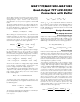
Low-Dropout Linear Regulator (MAX1778/
MAX1881/MAX1883/MAX1884 Only)
Output-Voltage Selection
Adjust the linear-regulator output voltage by connecting
a voltage-divider from LDOOUT to FBL to GND
(Figure 5). Select R8 in the 5kΩ to 50kΩ range. Calculate
R7 with the following equation:
R7 = R8 [(V
LDOOUT
/V
FBL
) - 1]
where V
FBL
= 1.25V, and V
LDOOUT
can range from
1.25V to (V
SUPL
- 300mV). FBL’s input bias current is
0.8µA (max). For less than 0.5% error due to FBL input
bias current (I
F
BL
), R8 must be less than 8kΩ.
C
I
fV
OUT
LOAD
CHP RIPPLE
≥
VVN
CXN NEG SUPN()
.( )> 15
VVVN
CXN POS SUPD SUPP()
. ( )>+
[]
15 1-
η
NEG
V
VN
NEG
SUPN
≅
η
POS
V
VVN
POS
SUPD SUPP
≅
+