
Datasheet


MAX1778/MAX1880–MAX1885
Quad-Output TFT LCD DC/DC
Converters with Buffer
28
Maxim Integrated
Charge-Pump Input Power and
Efficiency Considerations
The charge pumps in the MAX1778/MAX1880–MAX1882
provide regulated output voltages by controlling the
voltage drop across the low-side n-channel MOSFET, so
they can be modeled as linear regulators followed by an
unregulated charge pump when determining the input
power requirements and efficiency.
The charge pump only provides charge to the output
capacitor during half the period (50% duty cycle), so
the input current is a function of the number of stages
and the load current:
for the positive charge pump, and:
for the negative charge pump, where N is the number
of charge-pump stages.
The efficiency characteristics of the MAX1778/
MAX1880–MAX1882 regulated charge pumps are simi-
lar to a linear regulator. It is dominated by quiescent
current at low output currents and by the input voltage
IIN
SUPP POS
() =+1
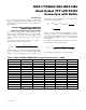
CIRCUIT 6 CIRCUIT 7 CIRCUIT 8 CIRCUIT 9
V
IN
3.3V 3.3V 3.3V 3.3V
V
MAIN
9V 9V 9V 9V
I
MAIN(MAX)
100mA 100mA 200mA 200mA
V
NEG
-5V -5V -5V -5V
I
NEG
2mA 2mA 5mA 5mA
V
POS
24V 24V 24V 24V
I
POS
2mA 2mA 5mA 5mA
L 4.7µH 10µH 10µH 10µH
I
PEAK
>1A >1A >1A >1A
C
OUT
4.7µF 10µF 10µF 20µF
R1 309kΩ 309kΩ 309kΩ 309kΩ
R2 49.9kΩ 49.9kΩ 49.9kΩ 49.9kΩ
R
COMP
None None None 20kΩ*
C
COMP
None None None 200pF*
Table 2. MAX1881/MAX1882/MAX1884/MAX1885 Component Values (f
OSC
= 500kHz)
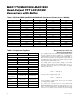
SUPPLIER PHONE FAX
INDUCTORS
Coilcraft 847-639-6400 847-639-1469
Coiltronics 561-241-7876 561-241-9339
Sumida USA 847-956-0666 847-956-0702
TOKO 847-297-0070 847-699-1194
CAPACITORS
AVX 803-946-0690 803-626-3123
KEMET 408-986-0424 408-986-1442
SANYO 619-661-6835 619-661-1055
Taiyo Yuden 408-573-4150 408-573-4159
DIODES
Central
Semiconductor
516-435-1110 516-435-1824
International
Rectifier
310-322-3331 310-322-3332
Motorola 602-303-5454 602-994-6430
Nihon 847-843-7500 847-843-2798
Zetex 516-543-7100 516-864-7630
Table 3. Component Suppliers
*R
COMP
and C
COMP
are connected between the step-up converter’s output (V
MAIN
) and FB.
IIN
SUPP POS
() =+1