
Datasheet


MAX1778/MAX1880–MAX1885
Quad-Output TFT LCD DC/DC
Converters with Buffer
22
Maxim Integrated
Negative Charge Pump
During the first half-cycle, the p-channel MOSFET turns
on, and flying capacitor C
X(NEG)
charges to V
SUPN
minus a diode drop (Figure 4). During the second
half-cycle, the p-channel MOSFET turns off, and the
n-channel MOSFET turns on, level shifting C
X(NEG)
.
This connects C
X(NEG)
in parallel with reservoir capaci-
tor C
OUT(NEG)
. If the voltage across C
OUT(NEG)
minus
a diode drop is greater than the voltage across
C
X(NEG)
, charge flows from C
OUT(NEG)
to C
X(NEG)
until
the diode (D5) turns off. The amount of charge trans-
ferred to the output is controlled by the variable
n-channel on-resistance.
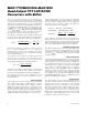
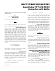
Low-Dropout Linear Regulator (MAX1778/
MAX1881/MAX1883/MAX1884 Only)
The MAX1778/MAX1881/MAX1883/MAX1884 contain a
low-dropout linear regulator (Figure 5) that uses an
internal PNP pass transistor (Q
P
) to supply loads up to
40mA. As illustrated in Figure 5, the 1.25V reference is
connected to the error amplifier, which compares this
reference with the feedback voltage and amplifies the
difference. If the feedback voltage is higher than the
reference voltage, the controller lowers the base
current of Q
P
, which reduces the amount of current to
the output. If the feedback voltage is too low, the
device increases the pass transistor base current,
which allows more current to pass to the output and
increases the output voltage. However, the linear regu-
lator also includes an output current limit to protect the
internal pass transistor against short circuits.
The low-dropout linear regulator monitors and controls
the pass transistor’s base current, limiting the output
current to 130mA (typ). In conjunction with the thermal
overload protection, this current limit protects the
output, allowing it to be shorted to ground for an indefi-
nite period of time without damaging the part.
VCOM Buffer
The MAX1778/MAX1880–MAX1885 include a VCOM
buffer, which uses an operational transconductance
amplifier (OTA) to provide a current output that is ideal
for driving capacitive loads, such as the backplane of a
TFT LCD panel. The unity-gain bandwidth of this
current-output buffer is:
GBW = gm/C
OUT
where gm is the amplifier’s transconductance. The
bandwidth is inversely proportional to the output
capacitor, so large capacitive loads improve stability;
however, lower bandwidth decreases the buffer’s tran-
sient response time. To improve the transient response
SUPL
C
SUPL
V
SUPL
4.5V TO 15V
C
LDOOUT
LDOOUT
V
LDOOUT
1.25V TO (V
SUPL
- 0.3V)
FBL
V
REF
1.25V
ERROR
AMPLIFIER
GND
R8
R7
Q
P
CURRENT
LIMIT
THERMAL
SENSOR
V
LDOOUT
=
(
1 +
)
V
REF
V
REF
= 1.25V
R7
R8
MAX1778
MAX1881
MAX1883
MAX1884
Figure 5. Low-Dropout Linear Regulator Block Diagram