
Datasheet


MAX1778/MAX1880–MAX1885
Quad-Output TFT LCD DC/DC
Converters with Buffer
21
Maxim Integrated
The switching waveforms appear noisy and asynchro-
nous when light loading causes pulse-skipping opera-
tion; this is a normal operating condition that improves
light-load efficiency.
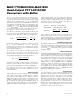
Dual Charge-Pump Regulator (MAX1778/
MAX1880–MAX1882 Only)
The MAX1778/MAX1880–MAX1882 controllers contain
two independent low-power charge pumps (Figure 4).
One charge pump inverts the input voltage and pro-
vides a regulated negative output voltage. The second
charge pump doubles the input voltage and provides a
regulated positive output voltage. The controllers
contain internal p-channel and n-channel MOSFETs to
control the power transfer. The internal MOSFETs
switch at a constant frequency (fCHP = fOSC/2).
Positive Charge Pump
During the first half-cycle, the n-channel MOSFET turns
on and charges flying capacitor C
X(POS)
(Figure 4).
This initial charge is controlled by the variable
n-channel on-resistance. During the second half-cycle,
the n-channel MOSFET turns off and the p-channel
MOSFET turns on, level shifting C
X(POS)
by V
SUPP
volts.
This connects C
X(POS)
in parallel with the reservoir
capacitor C
OUT(POS)
. If the voltage across C
OUT(POS)
plus a diode drop (V
POS
+ V
DIODE
) is smaller than the
level-shifted flying capacitor voltage (V
CX(POS)
+
V
SUPP
), charge flows from C
X(POS)
to C
OUT(POS)
until
the diode (D3) turns off.
INDUCTOR CURRENT
I
LOAD
t
ON
t
OFF
TIME
I
PEAK
Figure 3. Discontinuous-to-Continuous Conduction Crossover
Point
MAX1778
MAX1880
MAX1881
MAX1882
V
NEG
= - V
REF
V
REF
= 1.25V
( )
R5
R6
R5
R6
C
OUT(NEG)
C
X(NEG)
V
SUPN
2.7V TO 13V
OSC
REF
PGNDGND
SUPN
DRVN
FBN
SUPP
DRVP
FBP
D4
D5
V
POS
= 1 + V
REF
V
REF
= 1.25V
R3
R4
( )
V
SUPP
2.7V TO 13V
V
SUPD
D2
D3
C
REF
0.22µF
V
REF
1.25V
R4
C
X(POS)
C
OUT(POS)
V
POS
V
NEG
R3
Figure 4. Low-Power Charge Pump Block Diagram