
Datasheet


MAX1761
Small, Dual, High-Efficiency
Buck Controller for Notebooks
8 _______________________________________________________________________________________
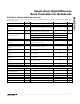
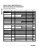
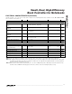
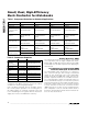
PIN NAME FUNCTION
1 FB1
Feed b ack Inp ut for the 2.5V P WM . C onnect FB1 to GN D for a fi xed 2.5V outp ut. C onnect a r esi sti ve
vol tag e- d i vi d er to FB1 to ad j ust OU T1 fr om 1V to 5.5V . FB1 r eg ul ates to 1V ( see Ad j usti ng V
OUT
secti on) .
2 OUT1
Output Voltage Connection for PWM1. OUT1 senses the output voltage to set the regulator on-time
and is connected internally to a 160kΩ feedback input in fixed-output mode.
3 REF
2V Reference Voltage Output. Bypass REF to GND with 0.1µF (min) capacitor. Can supply 50µA for
external loads.
When ON1 = High, Normal/Forced PWM Mode Selection and OUT2 On/Off Control Input
ON2 CONDITION MODE SELECTED
LOW (ON2 < 0.5V) OUT1 is enabled in normal mode; OUT2 is shut down.
HIGH (2V < ON2 < VL) Both outputs are enabled in normal mode.
4 ON2
Floating Both outputs are enabled in forced-PWM mode.
5V+
Battery Voltage. V+ is the input for the VL regulator and DH gate drivers and is also used for PWM
one-shot timing.
6 ON1
On/Off Control Input. Drive ON1 high to enable the device. Drive ON1 low to enter micropower
shutdown mode. Both REF and VL are disabled in shutdown. ON1 may be pinstrapped to V+.
7 OUT2
Output Voltage Connection for PWM2. OUT2 senses the output voltage to set the regulator on-time
and is connected internally to a 160kΩ feedback input in fixed-output mode.
8 FB2
Feed b ack Inp ut for the 1.8V P WM . C onnect FB2 to GN D for a fi xed 1.8V outp ut. C onnect a r esi sti ve
vol tag e- d i vi d er to FB2 to ad j ust OU T2 fr om 1V to 5.5V . FB2 r eg ul ates to 1V ( see Ad j usti ng V
OU T
secti on) .
9 DH2 High-Side Gate Driver Output for PWM2. Swings between GND and V+.
10 CS2
Current-Sense Connection for PWM2. Connect CS2 to the drain of the low-side driver. Alternatively,
connect CS2 to the junction of the source of the low-side FET and a current-sense resistor to GND.
11 DL2 Low-Side Gate Driver Output for PWM2. DL2 swings between GND and VL.
12 GND Combined Power and Analog Ground
13 VL
Linear Regulator Output. VL is the output of the 4.65V internal linear regulator, capable of supplying
25mA for external loads. The VL pin also serves as the supply input for the DL gate driver and the
analog/logic blocks. VL can be overdriven by an external 5V supply to improve efficiency. Bypass
VL to GND with a 4.7µF ceramic capacitor.
14 DL1 Low-Side Gate Driver Output for PWM1. DL1 swings between GND and VL.
15 CS1
Current-Sense Connection for PWM1. Connect CS1 to the drain of the low-side driver. Alternatively,
connect CS1 to the junction of the source of the low-side FET and a current-sense resistor to GND.
16 DH1 High-Side Gate Driver Output for PWM1. DH1 swings between GND and V+.
Pin Description