
Datasheet


MAX1761
Small, Dual, High-Efficiency
Buck Controller for Notebooks
_______________________________________________________________________________________ 5
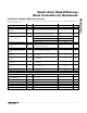
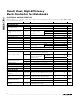
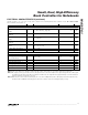
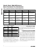
PARAMETER SYMBOL CONDITIONS MIN TYP MAX UNITS
GATE DRIVERS
DH_ Gate Driver On-Resistance
(Pullup)
V+ = 6V to 20V, DH_, high state 8 Ω
DH_ Gate Driver On-Resistance
(Pulldown)
DH_, low state 10 Ω
DL_ Gate Driver On-Resistance
(Pullup)
DL_, high state 8 Ω
DL_ Gate Driver On-Resistance
(Pulldown)
DL_, low state 5 Ω
DH_ Gate Driver Source/Sink
Current
V
DH_
= 3V, V+ = 6V A
DL_ Gate Drive Sink Current V
DL_
= 2.5V A
DL_ Gate Driver Source Current V
DL_
= 2.5V A
LOGIC CONTROLS
ON_ Logic Input High Voltage 2.05 V
ON2 Logic Input Float Voltage
(Forced-PWM Mode)
V
ON1
> 2.0V 1.3 1.95 V
ON_ Logic Input Low Voltage 0.5 V
ON1 Logic Input Current -1 1 µA
ON2 Logic High Input Current V
ON2
> 2.0V 0 3 µA
ON2 Logic Low Input Current V
ON2
< 0.5V, V
ON1
> 2.0V -2 0 µA
FB_ Dual Mode Threshold 50 150 mV
ELECTRICAL CHARACTERISTICS (continued)
(Circuit of Figure 1, V+ = 15V, C
VL
= 4.7µF, C
REF
= 0.1µF, VL not externally driven unless otherwise noted, T
A
= -40°C to +85°C,
unless otherwise noted.) (Note 1)
Note 1: Specifications to -40°C are guaranteed by design, not production tested.
Note 2: If V+ is less than 5V, V+ must be connected to VL. If VL is connected to V+, V+ must be between 4.5V and 5.5V.
Note 3: DC output accuracy specifications refer to the trip-level error of the error amplifier. The output voltage will have a DC regula-
tion higher than the trip level by 50% of the ripple. In PFM mode, the output will rise by approximately 1.5% when transition-
ing from continuous conduction to no load.
Note 4: One-shot times are measured at the DH pin (V+ = 15V, C
DH
= 400pF, 90% point to 90% point). Actual in-circuit times may
be different due to MOSFET switching speeds.This effect can also cause the switching frequency to vary.