
Datasheet


MAX1761
Small, Dual, High-Efficiency
Buck Controller for Notebooks
2 _______________________________________________________________________________________
ABSOLUTE MAXIMUM RATINGS
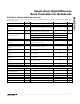
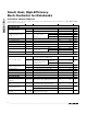
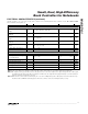
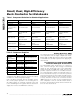
ELECTRICAL CHARACTERISTICS
(Circuit of Figure 1, V+ = 15V, C
VL
= 4.7µF, C
REF
= 0.1µF, VL not externally driven unless otherwise noted, T
A
= 0°C to +85°C, unless
otherwise noted.) (Note 1)
Stresses beyond those listed under “Absolute Maximum Ratings” may cause permanent damage to the device. These are stress ratings only, and functional
operation of the device at these or any other conditions beyond those indicated in the operational sections of the specifications is not implied. Exposure to
absolute maximum rating conditions for extended periods may affect device reliability.
V+ to GND ..............................................................-0.3V to +22V
VL to GND ................................................................-0.3V to +6V
VL to V+ .............................................................................+0.3V
OUT_, ON2 to GND ..................................................-0.3V to +6V
ON1, DH_ to GND ........................................-0.3V to (V+ + 0.3V)
FB_, REF, DL_ to GND.................................-0.3V to (VL + 0.3V)
CS_ to GND .....................................................-2V to (V+ + 0.3V)
REF Short Circuit to GND ...........................................Continuous
Continuous Power Dissipation
16-Pin QSOP (derate 8.3mW/°C above +70°C) ......….667mW
Operating Temperature Range ...........................-40°C to +85°C
Junction Temperature......................................................+150°C
Storage Temperature.........................................-65°C to +150°C
Lead Temperature (soldering, 10s) .................................+300°C
PARAMETER SYMBOL CONDITIONS MIN TYP MAX UNITS
PWM CONTROLLERS
Input Voltage Range V+ (Note 2) 4.5 20 V
FB_ = OUT_ 0.99 1 1.01
FB1 = GND 2.475 2.5 2.525 V
DC Output Voltage Accuracy
(Note 3)
V
OUT_
V+
= 4.5V to 20V,
VL
= 4.75V to 5.25V,
ON2 = VL
FB2 = GND 1.782 1.8 1.818
Output Voltage Adjust Range 1 5.5 V
OUT_ Input Resistance 80 160 300 kΩ
FB_ Input Bias Current V
FB_
= 1V, VL = 5V -0.1 0.1 µA
CS_ Input Bias Current V
CS_
= 0, VL = 5V -1 1 µA
Soft-Start Ramp Time Zero to full ILIM 1700 µs
OUT1 661 735 809
On-Time (Note 4) t
ON
V+
= 10V, V
OUT1
= 2.5V,
V
OUT2
= 1.8V
OUT2 648 720 792
ns
Minimum Off-Time (Note 4) t
OFF
400 500 ns
BIAS AND REFERENCE
IL
FB1 = FB2 = GND, VL = 5V, V
OUT1
and
V
OUT2
forced above regulation point
0.60 1.20 mA
VL undriven 0.95 1.70
Quiescent Supply Current
I+
FB1 = FB2 = GND, V
OUT1
and V
OUT2
forced
above regulation point
VL = 5V 0.38 0.65
mA
IL VL = 5V, ON1 = ON2 = GND 5 10 µA
Shutdown Supply Current
I+ VL = 0, 5V 4 10 µA
VL Output Voltage VL I
LOAD
= 0 to 25mA, V+ = 5V to 20V 4.5 4.65 4.75 V
Reference Voltage V
REF
V+ = 5V to 20V, no load 1.98 2 2.02 V
Reference Load Regulation I
REF
I
REF
= 0 to 50µA 8 mV
REF Sink Current REF in regulation 10 µA
Falling edge 1.6
REF Fault Lockout Voltage
Rising edge 1.94
V