
Datasheet


MAX1761
Small, Dual, High-Efficiency
Buck Controller for Notebooks
______________________________________________________________________________________ 19
where I
LIMIT(MAX)
is the maximum valley current
allowed by the current-limit circuit, including threshold
tolerance and on-resistance variation. This means that
the MOSFETs must be very well heatsinked. If short-cir-
cuit protection without overload protection is enough, a
normal I
LOAD
value can be used for calculating compo-
nent stresses.
Choose a Schottky diode (D1, Figure 2) having a for-
ward voltage low enough to prevent the Q2 MOSFET
body diode from turning on during the dead time. As a
general rule, a diode having a DC current rating equal
to 1/3 of the load current is sufficient. This diode is
optional and can be removed if efficiency isn’t critical.
Applications Issues
Dropout Performance
The output voltage adjust range for continuous-conduc-
tion operation is restricted by the nonadjustable 500ns
(max) minimum off-time one-shot. For best dropout per-
formance, use the side with the lower switching fre-
quency, FB2 (250kHz). When working with low input
voltages, the duty-factor limit must be calculated using
worst-case values for on- and off-times. Manufacturing
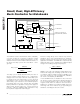
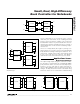
DH2
DH1
S
G
S
D
D
D
DG
DL1
V+
DG
DS
DS
DS
P-CHANNEL
P-CHANNEL
LX1
LX2
N-CHANNEL
1
1
DL2DG
DS
DS
DS
N-CHANNEL
1
Figure 9. Two Single N-Channel MOSFETs and a Dual P-Channel
MOSFET Design
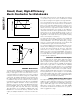
DH1
S
S
S
D
D
D
DG
LX1
DL1
V+
DG
DS
DS
DS
DH2
S
S
S
D
D
D
DG
LX2
DL2
V+
DG
DS
DS
DS
P-CHANNEL N-CHANNEL P-CHANNEL N-CHANNEL
1
1
1
1
Figure 10. Two Single N-Channel MOSFETs and Two Single P-Channel MOSFETs Design
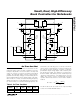
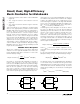
P-CHANNEL
DH1
V+
LX1
SD
GD
SD
GD
P-CHANNEL
DH2
1
LX2
N-CHANNEL
DL1
DL2
DG
DS
DG
DS
N-CHANNEL
1
Figure 8. Dual N- and P-Channel MOSFET Design