
Datasheet


MAX1761
Small, Dual, High-Efficiency
Buck Controller for Notebooks
12 ______________________________________________________________________________________
The maximum on-time and minimum off-time, t
OFF(MIN)
,
one-shots restrict the continuous-conduction output
voltage. The worst-case dropout performance occurs
with the minimum on-time and the maximum off-time, so
the worst-case duty cycle for V
IN
= 6V, V
OUT1
= 5V is
given by:
The duty cycle is ideally determined by the ratio of
input-to-output voltage (Duty Cycle = V
OUT
/V
IN
).
Voltage losses in the loop cause the actual duty cycle
to deviate from this relationship. See the Dropout
Performance section for more information. Equate the
off-time duty cycle restriction to the nonideal input/out-
put voltage duty cycle ratio. Typical units will exhibit
better performance. Operation of any power supply in
dropout will greatly reduce the circuit’s transient
response, and some additional bulk capacitance may
be required to support fast load changes.
Resistive voltage drops in the inductor loop and the
dead-time effect cause switching-frequency variations.
Parasitic voltage losses decrease the effective voltage
applied to the inductor. The MAX1761 compensates by
shifting the duty cycle to maintain the regulated output
voltage. The resulting change in frequency is:
V
DROP1
is the sum of the parasitic voltage drops in the
inductor discharge path, including synchronous rectifi-
er, inductor, and PC board resistances; V
DROP2
is the
sum of the resistances in the charging path; and t
ON
is
the on-time calculated by the MAX1761.
In forced PWM mode, the dead-time effect increases
the effective on-time, reducing the switching frequency
as one or both dead times. This occurs only at light or
negative loads when the inductor current reverses.
Under these conditions, the inductor’s EMF causes the
switching node of the inductor to go high during the
dead time, extending the effective on-time.
ƒ=
V+V
(V + V )
OUT DROP1
ON IN DROP2
t
Duty Cycle
t
t+ t
ON(MIN)
ON(MIN)
OFF(MAX)
==
+
=
2 054
2 054 500
80 4
.
.
.%
µ
µ
s
sns
OUT
REF
UVP
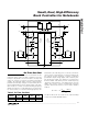
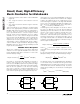
FROM ZERO-CROSSING DETECTOR
FROM CURRENT-LIMIT COMPARATOR
ERROR
AMP
TOFF
TON
REF
-30%
FEEDBACK
MUX
(SEE FIGURE 12)
x2
TO DL DRIVER INPUT
FROM OUT
FROM FEEDBACK
TO DH DRIVER INPUT
ON-TIME
COMPUTE
TON
1-SHOT
1-SHOT
1-SHOT
TRIG
TRIG
Q
Q
Q
S
R
FB
OUT
GAIN
DRIVER
Q
TIMER
SHDN
SHDN
ON/OFF
CONTROL
V
IN
S
R
Q
UVP
LATCH
MAX1761
Figure 3. PWM Controller (One Side Only)