
Datasheet

10
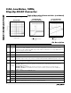
ON MAX1760H Enable Input. When ON is high, the IC is on. Connect to OUT for normal operation.
MAX1760/MAX1760H
0.8A, Low-Noise, 1MHz,
Step-Up DC-DC Converter
6 _______________________________________________________________________________________
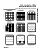
NOISE SPECTRUM
MAX1760-13
1010.1
16
4
0
12
8
FREQUENCY (MHz)
NOISE (mV
RMS
)
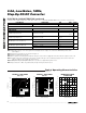
TURN-ON WAVEFORMS
NO SOFT-START COMPONENTS
MAX1760-14
OV
C
A
B
t = 2ms/div
A = ON, 5V/div
B = INPUT CURRENT, 500mA/div
C = V
OUT
, 2V/div
SOFT-START WAVEFORMS
R
SS
= 500kΩ, C
SS
= 0.1µF
MAX1760-15
0V
C
A
B
2.00ms/div
A = ON, 5V/div
B = INPUT CURRENT, 100mA/div
C = V
OUT
, 2V/div
Pin Description
Typical Operating Characteristics (continued)
(Circuit of Figure 2, V
IN
= 2.4V, V
OUT
= 3.3V, T
A
= +25°C, unless otherwise noted.)
NAME
FUNCTION
1 ISET
N-Channel Current-Limit Control. For maximum current limit, connect to REF. To reduce current, supply a
voltage between REF and GND by means of a resistive voltage-divider. If soft-start is desired, connect a
capacitor from ISET to GND. When ON = high, or V
REF
<80% of nominal value, an on-chip 100kΩ switched
resistor discharges this pin to GND.
2 REF
1.250V Voltage Reference Bypass. Connect a 0.22µF ceramic bypass capacitor to GND. Up to 50µA of
external load current is allowed.
PIN
3 GND Ground. Connect to PGND with short trace.
4 FB
DC-DC Converter Feedback Input. To set fixed output voltage of +3.3V, connect FB to ground. For
adjustable output of 2.5V to 5.5V, connect to a resistive divider from OUT to GND. FB set point = 1.24V.
8 LX Inductor Connection
7 PGND Source of N-Channel Power MOSFET Switch
6 CLK/SEL
Clock Input for the DC-DC Converter. Also serves to program operating mode of switcher as follows:
CLK/SEL = LO: Normal operation—operates at a fixed frequency, automatically switching to low-power
mode if load is minimized.
CLK/SEL = HI: Forced-PWM mode—operates in low-noise, constant-frequency mode at all loads.
CLK/SEL = Clocked: Forced-PWM mode with the internal oscillator synchronized to CLK in 500kHz to
1200kHz range.
5 OUT
IC Power, Supplied from the Output. Bypass to GND with a 0.68µF ceramic capacitor, and connect to POUT
with a series 4.7Ω resistor (Figure 2).
9 POUT Power Output. P-channel synchronous-rectifier source.
— EP
Exposed Paddle (TDFN Package Only). Internally connected to GND. Connect to a large ground plane to
maximize thermal dissipation. Do not use as sole ground connection.
ON MAX1760 Enable Input. When ON is low, the IC is on. Connect to GND for normal operation.