
Datasheet
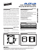
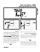
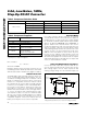

MAX1760/MAX1760H
0.8A, Low-Noise, 1MHz,
Step-Up DC-DC Converter
2 _______________________________________________________________________________________
ABSOLUTE MAXIMUM RATINGS
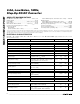
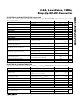
ELECTRICAL CHARACTERISTICS
(CLK/SEL = FB = PGND = GND, ISET = REF, OUT = POUT, V
OUT
= 3.6V, T
A
= 0°C to +85°C. Typical values are at T
A
= +25°C,
unless otherwise noted.)
Stresses beyond those listed under “Absolute Maximum Ratings” may cause permanent damage to the device. These are stress ratings only, and functional
operation of the device at these or any other conditions beyond those indicated in the operational sections of the specifications is not implied. Exposure to
absolute maximum rating conditions for extended periods may affect device reliability.
ON, ON, OUT, CLK/SEL to GND ..................................-0.3V to +6V
PGND to GND ..........................................................................±0.3V
LX to PGND .................................................-0.3V to (V
POUT
+ 0.3V)
POUT to OUT ...........................................................................±0.3V
REF, FB, ISET, POUT to GND.......................-0.3V to (V
OUT
+ 0.3V)
Continuous Power Dissipation (T
A
= +70°C)
Single-Layer Board:
10-Pin µMAX
(derate 5.6mW/°C above +70°C).................................….444mW
10-Pin TDFN-EP (derate 18.5mW/°C above +70°C) .....1482mW
Multilayer Board:
10-Pin µMAX (derate 8.8mW/°C above +70°C) ..........….707mW
10-Pin TDFN-EP (derate 24.4mW/°C above +70°C) .....1951mW
Operating Temperature Range................................-40°C to +85°C
Junction Temperature ...........................................................+150°C
Storage Temperature Range .................................-65°C to +150°C
Lead Temperature (soldering, 10s)......................................+300°C
PARAMETER CONDITIONS
MIN TYP MAX
UNITS
DC-DC CONVERTER
Input Voltage Range (Note 1) 0.7 5.5 V
Minimum Startup Voltage I
LOAD
< 1mA, T
A
= +25°C (Note 2) 0.9 1.1 V
Temperature Coefficient of Startup Voltage I
LOAD
< 1mA
-2.3
mV/°C
Frequency in Startup Mode V
OUT
= 1.5V
125 500 1000
kHz
Internal Oscillator Frequency CLK/SEL = OUT 0.8 1 1.2
MHz
Oscillator Maximum Duty Cycle (Note 3) 80 86 90 %
External Clock Frequency Range 0.5 1.2
MHz
Output Voltage
V
FB
< 0.1V, CLK/SEL = OUT, includes load
regulation for 0 < I
LX
< 0.55A
3.17
3.3
3.38
V
FB Regulation Voltage
Adjustable output, CLK/SEL = OUT, includes
load regulation for 0 < I
LX
< 0.55A
1.215 1.240 1.270
V
FB Input Leakage Current
V
FB
= 1.35V (T
A
= +25°C, MAX1760ETB,
MAX1760HETB)
0.01 100
nA
Load Regulation
CLK/SEL = OUT, no load to full load
(0 < I
LX
< 1.0A)
-1.5
%
Output Voltage Adjust Range 2.5 5.5 V
Output Voltage Lockout Threshold Rising edge (Note 4)
2.00 2.15 2.30
V
ISET Input Leakage Current
V
ISET
= 1.25V (T
A
= +25°C, MAX1760ETB,
MAX1760HETB)
±0.01 ±50
nA
Supply Current in Shutdown V
ON
= 3.6V, V
ON
= 0V 0.1 5 µA
No-Load Supply Current CLK/SEL = GND (Note 5)
100 185
µA
No-Load Supply Current Forced-PWM Mode
CLK/SEL = OUT 2.5
mA
DC-DC SWITCHES
POUT Leakage Current
V
LX
= 0, V
OUT
= 5.5V (T
A
= +25°C,
MAX1760ETB, MAX1760HETB)
0.1 10 µA
LX Leakage Current
V
LX
= V
OUT
= 5.5V, in shutdown (T
A
=
+25°C, MAX1760ETB, MAX1760HETB)
0.1 10 µA