
Datasheet

MAX17014
Low-Cost Multiple-Output
Power Supply for LCD TVs
4 _______________________________________________________________________________________
ELECTRICAL CHARACTERISTICS (continued)
(Circuit of Figure 1, V
IN
= V
IN2
= 12V, AV
DD
= V
OVIN
= V
SUP
= 15V, T
A
= 0°C to +85°C. Typical values are at T
A
= +25°C, unless oth-
erwise noted.)
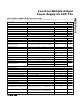
PARAMETER CONDITIONS MIN TYP MAX UNITS
FB1 Load Regulation 0 < I
LOAD
< full, transient only -1 %
FB1 Line Regulation 10.8V < V
VIN
< 13.2V 0.08 0.15 %/V
FB1 Input Bias Current V
FB1
= 1.25V 25 125 200 nA
FB1 Transconductance I = ±2.5μA at COMP, FB1 = COMP 150 320 560 μS
FB1 Voltage Gain FB1 to COMP 1400 V/V
LX1 Leakage Current V
FB1
= 1.5V, V
LX1
= 20V 4 40 μA
LX1 Current Limit V
FB1
= 1.1V, duty cycle = 25% 3.2 3.7 4.2 A
Current-Sense Transresistance 0.16 0.23 0.30 V/A
LX1 On-Resistance 110 220 m
Soft-Start Period 3 ms
Soft-Start Step Size
I
LIM
/
128
A
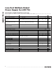
POSITIVE AND NEGATIVE CHARGE-PUMP REGULATORS
SUP Input Supply Range 8.0 18.0 V
SUP Input Supply Current V
FBP
= 1.5V, V
FBN
= 0.15V (not switching) 0.2 0.4 mA
SUP Overvoltage Threshold SUP rising edge, 250mV typical hysteresis (Note 3) 18 19 20 V
0°C < T
A
< +85°C
1.23 1.25 1.27
FBP Regulation Voltage
T
A
= +25°C 1.2375 1.2625
V
FBP Line-Regulation Error 11V < V
SUP
< 16V, not in dropout 0.2 %/V
FBP Input Bias Current V
FBP
= 1.5V -50 +50 nA
DRVP p-Channel MOSFET
On-Resistance
1.0 3.0
DRVP n-Channel MOSFET
On-Resistance
0.5 1.0
FBP Fault Trip Level Falling edge 0.96 1.00 1.04 V
Positive Charge-Pump Soft-Start Period 3 ms
Positive Charge-Pump Soft-Start
Step Size
V
REF
/
128
V
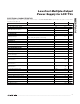
0°C < T
A
< +85°C 0.988 1.000 1.012
FBN Regulation Voltage V
REF
- V
FBN
T
A
= +25°C 0.99 1.00 1.01
V
FBN Input Bias Current V
FBN
= 0mV -50 +50 nA
FBN Line Regulation Error 11V < V
SUP
< 16V, not in dropout 0.2 %/V
DRVN p-Channel On-Resistance 1.0 3.0
DRVN n-Channel On-Resistance 0.5 1.0
FBN Fault Trip Level Rising edge 450 500 550 mV
Negative Charge-Pump Soft-Start
3 ms
Negative Charge-Pump Soft-Start
Step Size
(V
REF
-
V
FBN
) /
128
V