
Datasheet

• Place all feedback voltage-divider resistors as
close to their respective feedback pins as possible.
The divider’s center trace should be kept short.
Placing the resistors far away causes their FB
traces to become antennas that can pick up switch-
ing noise. Care should be taken to avoid running
any feedback trace near LX1, LX2, DRVP, or DRVN.
• Place V
IN
pin, VL pin, and REF pin bypass capaci-
tors as close to the device as possible. The ground
connection of the VL bypass capacitor should be
connected directly to the GND pin with a wide trace.
• Minimize the length and maximize the width of the
traces between the output capacitors and the load
for best transient responses.
• Minimize the size of the LX1 and LX2 nodes while
keeping them wide and short. Keep the LX1 and
LX2 nodes away from feedback nodes (FB1, FB2,
FBP, and FBN) and analog ground. Use DC traces
as a shield, if necessary.
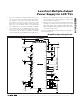
Refer to the MAX17014 evaluation kit for an example of
proper board layout.
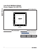
MAX17014
Low-Cost Multiple-Output
Power Supply for LCD TVs
______________________________________________________________________________________ 31
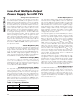
LX2
REF
FB1
LX1
LX1
GND
COMP
V
IN
OUT
AV
DD
FSEL
FB2
OUT
ON/OFF
ON/OFF
VL
V
IN
V
IN
GON
OVIN
OGND
VL
REF
BST
GON
DRN
CTL
SWI
GON CONTROL
DRVN
FBN
CPGND
REF
DRVP
FBP
SUP
SRC
GND1
GND1
NEG2
OUT2
VCOM1
DEL1
DEL2
EN1
EN2
NEG1
OUT1
SWI
SWO
SUI
POS1
THR
POS2
DLP
MODE
AV
DD
VCOM2
SWI
SRC
AV
DD
IN2
IN2
LX2
GOFF
MAX17014
EP
Simplified Operating Circuit