
Datasheet

MAX17014
Low-Cost Multiple-Output
Power Supply for LCD TVs
2 _______________________________________________________________________________________
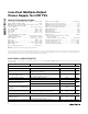
ABSOLUTE MAXIMUM RATINGS
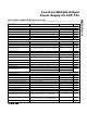
ELECTRICAL CHARACTERISTICS
(Circuit of Figure 1, V
IN
= V
IN2
= 12V, AV
DD
= V
OVIN
= V
SUP
= 15V, T
A
= 0°C to +85°C. Typical values are at T
A
= +25°C, unless oth-
erwise noted.)
Stresses beyond those listed under “Absolute Maximum Ratings” may cause permanent damage to the device. These are stress ratings only, and functional
operation of the device at these or any other conditions beyond those indicated in the operational sections of the specifications is not implied. Exposure to
absolute maximum rating conditions for extended periods may affect device reliability.
V
IN
, IN2, OVIN, SUP, EN1, EN2, FSEL to GND ......-0.3V to +22V
GND1, OGND, CPGND to GND .........................................±0.3V
MODE, DLP, CTL, THR, DEL1, DEL2, VL to GND ...-0.3V to +7.5V
REF, FBP, FBN, FB1, FB2, COMP,
OUT to GND ...........................................-0.3V to (V
VL
+ 0.3V)
SWI, SWO to GND ..................................................-0.3V to +22V
LX1 to GND1 ..........................................................-0.3V to +22V
SWI to SWO ............................................................-0.3V to +22V
SWI to SUI .............................................................-0.3V to +7.5V
POS1, NEG1, OUT1, POS2, NEG2,
OUT2 to OGND...................................-0.3V to (V
OVIN
+ 0.3V)
DRVN, DRVP to CPGND ...........................-0.3V to (V
SUP
+ 0.3V)
LX2 to CPGND ...........................................-0.3V to (V
IN2
+ 0.3V)
BST to VL................................................................-0.3V to +22V
SRC to GND ...........................................................-0.3V to +48V
GON, DRN to GND ...................................-0.3V to (V
SRC
+ 0.3V)
GON to DRN...........................................................-0.3V to +48V
POS_ to NEG_ RMS Current ...................................5mA (Note 1)
REF Short Circuit to GND ...........................................Continuous
RMS LX1 Current (total for both pins) ...................................3.2A
RMS GND1 Current (total for both pins) ...............................3.2A
RMS IN2 Current (total for both pins)....................................3.2A
RMS LX2 Current (total for both pins) ...................................3.2A
RMS CPGND Current............................................................0.8A
RMS SWI Current ..................................................................2.4A
RMS SWO Current ................................................................2.4A
RMS DRVN, DRVP Current ...................................................0.8A
RMS VL Current ..................................................................50mA
Continuous Power Dissipation (T
A
= +70°C)
48-Pin Thin QFN
(derate 38.5mW/°C above +70°C) .........................3076.9mW
Operating Temperature Range ...........................-40°C to +85°C
Junction Temperature......................................................+160°C
Storage Temperature Range .............................-65°C to +165°C
Soldering Temperature (reflow) .......................................+260°C
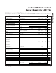
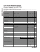
PARAMETER CONDITIONS MIN TYP MAX UNITS
GENERAL
V
IN
, IN2 Input Voltage Range 8.0 16.5 V
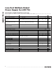
V
IN
+ IN2 Quiescent Current
Only LX2 switching (V
FB1
= V
FBP
= 1.5V, V
FBN
= 0);
EN1 = EN2 = VL, V
FSEL
= 0
8 mA
V
IN
+ IN2 Standby Current
LX2 not switching (V
FB1
= V
FB2
= V
FBP
= 1.5V,
V
FBN
= 0); EN1 = EN2 = VL, V
FSEL
= 0
2 mA
V
IN
+ IN2 Shutdown Current EN1 = EN2 = GND (shutdown) 300 μA
SUP + OVIN Shutdown Current EN1 = EN2 = GND (shutdown) 10 μA
FSEL = V
IN
1020 1200 1380
SMPS Operating Frequency
FSEL = GND 510 600 690
kHz
Phase Difference Between Step-
Down/Positive and Step-Up/Negative
Regulators
180 Degrees
V
IN
Undervoltage Lockout Threshold V
IN
rising edge, 100mV typical hysteresis 5.75 6.50 7.25 V
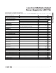
VL REGULATOR
VL Output Voltage
I
VL
= 25mA, V
FB1
= V
FB2
= V
FBP
= 1.1V, V
FBN
=
0.4V (all regulators switching)
4.9 5.0 5.1 V
VL Undervoltage Lockout Threshold VL rising edge, 100mV typical hysteresis 3.5 3.9 4.3 V
Note 1: See Figure 6 for the op amp clamp structures.