
Datasheet
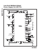
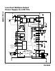

MAX17014
Low-Cost Multiple-Output
Power Supply for LCD TVs
______________________________________________________________________________________ 15
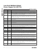
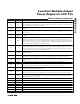
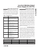
Pin Description (continued)
PIN NAME FUNCTION
23, 24 LX2
Step-Down Regulator Switching Node. LX2 is the source of the internal n-channel MOSFET
connected between IN2 and LX2. Connect the inductor and Schottky catch diode close to both LX2
pins to minimize the trace area for low EMI.
25, 26 IN2
Step-Down Regulator Power Input. Drain of the internal n-channel MOSFET connected between IN2
and LX2.
27 V
IN
Input of the Internal 5V Linear Regulator and the Startup Circuitry. Bypass V
IN
to GND with 0.22μF
close to the IC.
28 FSEL
Frequency-Select Pin. Connect FSEL to GND for 600kHz operation. Connect to VL or V
IN
for 1.2MHz
operation.
29 DEL2
Step-Up Regulator and Positive Charge-Pump Delay Input. Connect a capacitor from DEL2 and
GND to set the delay time between EN2 and the startup of these regulators, or between the step-
down startup and the startup of these regulators if EN1 is high before the step-down starts. An 8μA
current source charges C
DEL2
. DEL2 is internally pulled to GND through 10 resistance when EN1
or EN2 is low or when VL is below its UVLO threshold.
30 VL
5V Internal Linear Regulator Output. Bypass VL to GND with 1μF minimum. Provides power for the
internal MOSFET driving circuit, the PWM controllers, charge-pump regulators, logic, and reference
and other analog circuitry. Provides 25mA load current when all switching regulators are enabled.
VL is active whenever V
IN
is above V
IN
UVLO threshold.
31 COMP
Compensation Pin for the Step-Up Error Amplifier. Connect a series resistor and capacitor from
COMP to ground.
32 EN2
Step-Up and Positive Charge-Pump Regulator Enable Input. Input HIGH also enables DEL2 pullup
current. EN2 is inactive when EN1 is low. See the Power-Up Sequence section for details.
33 EN1
Step-Down and Negative Charge-Pump Regulator Enable Input. Input HIGH also enables DEL1
pullup current.
35, 36 GND1 Step-Up Regulator Power Ground. Source of the internal power n-channel MOSFET.
37, 38 LX1
Step-Up Regulator Power MOSFET n-Channel Drain and Switching Node. Connect the inductor and
Schottky catch diode to both LX1 pins and minimize the trace area for lowest EMI.
39 SWI
Step-Up Regulator Internal p-Channel MOSFET Pass Switch Source Input. Connect to the cathode of
the step-up regulator Schottky catch diode.
40 SUI
Step-Up Regulator Internal p-Channel MOSFET Pass Switch Gate Input. Connect a capacitor from
SUI to SWI to set the delay time. A 30μA current source pulls down on C
SUI
when DEL2 is high.
41 FB1
Boost Regulator Feedback Input. Connect FB1 to the center of a resistive voltage-divider between
the boost regulator output and GND to set the boost regulator output voltage. Place the resistive
voltage-divider within 5mm of FB1.
42 SWO Step-Up Regulator Internal p-Channel MOSFET Pass Switch Drain Output
43 OVIN Operational Amplifier Power Input
44 NEG2 Operational Amplifier 2 Inverting Input
45 POS2 Operational Amplifier 2 Noninverting Input
46 OUT2 Operational Amplifier Output 2
47 OGND Operational Amplifier Power Ground
48 NEG1 Operational Amplifier 1 Inverting Input
EP GND Exposed Paddle = GND