
Datasheet

MAX17014
Low-Cost Multiple-Output
Power Supply for LCD TVs
14 ______________________________________________________________________________________
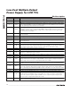
Pin Description
PIN NAME FUNCTION
1 POS1 Operational Amplifier 1 Noninverting Input
2 OUT1 Operational Amplifier 1 Output
3 THR
GON Low-Level Regulation Set-Point Input. Connect THR to the center of a resistive voltage-divider
between AV
DD
and GND to set the V
GON
falling regulation level. The regulation level is 10 x V
THR
.
See the High-Voltage Switch Control section for details.
4 MODE
High-Voltage Switch-Control Block Mode Selection Input and Timing-Adjustment Input. See the
High-Voltage Switch Control section for details. MODE is high impedance when it is connected to
VL. MODE is internally pulled to GND by a 10 resistor for 0.1μs typical when the high-voltage
switch-control block is enabled.
5 CTL
High-Voltage Switch-Control Block Timing Control Input. See the High-Voltage Switch Control
section for details.
6 DLP GON Output Enable. See the High-Voltage Switch Control section for details.
7 DRN Switch Input. Drain of the internal high-voltage p-channel MOSFET between DRN and GON.
8 GON
Internal High-Voltage MOSFET Switch Common Terminal. GON is the output of the high-voltage
switch-control block.
9 SRC Switch Input. Source of the internal high-voltage p-channel MOSFET between SRC and GON.
10 FBP
Positive Charge-Pump Regulator Feedback Input. Connect FBP to the center of a resistive voltage-
divider between the positive charge-pump regulator output and GND to set the positive charge-
pump regulator output voltage. Place the resistive voltage-divider within 5mm to FBP.
11 CPGND Charge Pump and Step-Down Regulator Power Ground
12 DRVP Positive Charge-Pump Driver Output. Connect DRVP to the positive charge-pump flying capacitor(s).
13 SUP
Supply Input for the Charge-Pump Drivers. Connect this pin to the output of the boost regulator SWI
and bypass to CPGND with a 0.1μF capacitor.
14 DRVN Negative Charge-Pump Driver Output. Connect DRVN to the negative charge-pump flying capacitor(s).
15, 34 GND Analog Ground
16 FBN
Negative Charge-Pump Regulator Feedback Input. Connect FBN to the center of a resistive
voltage-divider between the negative output and REF to set the negative charge-pump regulator
output voltage. Place the resistive voltage-divider within 5mm of FBN.
17 REF
Reference Output. Connect a 0.22μF capacitor from REF to GND. All power outputs are disabled
until REF exceeds its UVLO threshold. REF is active whenever V
IN
is above V
IN
UVLO threshold.
18 DEL1
Negative Charge-Pump Delay Input. Connect a capacitor from DEL1 and GND to set the delay time
between the step-down output and the negative output. An 8μA current source charges C
DEL1
.
DEL1 is internally pulled to GND through 10 resistance when EN1 is low or VL is below its UVLO.
19 N.C. No Connection. Not internally connected.
20 OUT Step-Down Regulator Output-Voltage Sense. Connect OUT to the step-down regulator output.
21 FB2
Step-Down Regulator Feedback Input. Connect FB2 to GND to select the step-down converter’s
3.3V fixed mode. For adjustable mode, connect FB2 to the center of a resistive voltage-divider
between the step-down regulator output and GND to set the step-down regulator output voltage.
Place the resistive voltage-divider within 5mm of FB2.
22 BST
Step-Down Regulator Bootstrap Capacitor Connection for High-Side Gate Driver. Connect a 0.1μF
ceramic capacitor from BST to LX2.