
Datasheet
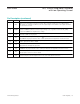

Pin Description
PIN NAME FUNCTION
1 SUP
Input Supply Voltage. SUP is the input voltage to the internal linear regulator. Bypass SUP to PGND with a
1μF minimum value ceramic capacitor.
2EN
Acti ve- H i g h E nab l e Inp ut. E N i s com p ati b l e w i th 5V and 3.3V l og i c l evel s. D r i ve E N l og i c- hi g h to enab l e the
output or drive EN logic-low to put the controller in low-power shutdown mode. Connect EN to SUP for
always-on operation. Do not leave EN unconnected.
3 FOSC
Oscillator-Timing Resistor Input. Connect a resistor from FOSC to SGND to set the oscillator frequency from
1MHz to 2.2MHz. See the Setting the Switching Frequency section.
4 FSYNC
Synchronization and Mode Selection Input. Connect FSYNC to BIAS to select fixed-frequency PWM mode
and disable skip mode. Connect FSYNC to SGND to select skip mode. Connect FSYNC to an external clock
for synchronization. FSYNC is internally pulled down to ground with a 1M_ resistor.
5 SGND
Signal Ground. Connect SGND directly to the local ground plane. Connect SGND to PGND at a single
point.
6 COMP
Error Amplifier Output. Connect COMP to the compensation feedback network. See the Compensation
Design section.
7FB
Feedback Regulation Point. Connect FB to BIAS for a fixed 5V output voltage. In adjustable mode, connect
to the center tap of a resistive divider from the output (V
OUT
) to SGND to set the output voltage. The FB
voltage regulates to 1V (typ).
8CS
Positive Current-Sense Input. Connect CS to the positive terminal of the current-sense element. Figure 4
shows two different current-sensing options: 1) accurate sense with a sense resistor or 2) lossless inductor
DCR sensing.
Maxim Integrated | 9www.maximintegrated.com
MAX16952
36V, 2.2MHz Step-Down Controller
with Low Operating Current
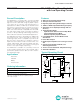
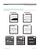
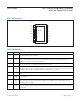
Pin Configuration
MAX16952
16
TSSOP
+
BST1SUP
15 DH2EN
14 LX3FOSC
13 BIAS4FSYNC
12 DL5SGND
11 PGND6COMP
10 PGOOD7FB
9
TOP VIEW
OUT8CS
EP