
Datasheet


MAX16952
Maxim Integrated | 22www.maximintegrated.com
36V, 2.2MHz Step-Down Controller
with Low Operating Current
Both n-channel MOSFETs must be logic-level types
with guaranteed on-resistance specifications at V
GS
=
4.5V. Ensure that the conduction losses at minimum
input voltage do not exceed MOSFET package thermal
limits or violate the overall thermal budget. Also, ensure
that the conduction losses, plus switching losses at the
maximum input voltage, do not exceed package ratings
or violate the overall thermal budget. The MAX16952’s
DL gate driver must drive the low-side MOSFET (NL). In
particular, check that the dV/dt caused by the high-side
MOSFET (NH) turning on does not pull up the NL gate
through its drain-to-gate capacitance. This is the most
frequent cause of cross-conduction problems.
Gate-charge losses are dissipated by the driver and do
not heat the MOSFET. Therefore, if the drive current is
taken from the internal LDO regulator, the power dissi-
pation due to drive losses must be checked. Both
MOSFETs must be selected so that their total gate
charge is low enough; therefore, BIAS can power both
drivers without overheating the IC:
P
DRIVE
= (V
SUP
- V
BIAS
) × Q
G_TOTAL
× f
SW
where Q
G_TOTAL
is the sum of the gate charges of both
MOSFETs.
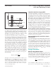
Boost-Flying Capacitor Selection
The bootstrap capacitor stores the gate voltage for the
internal switch. Its size is constrained by the switching
frequency and the gate charge of the high-side
MOSFET. Ideally the bootstrap capacitance should be
at least nine times the gate capacitance:
This results in a 10% voltage drop when the gate is
driven. However, if this value becomes too large to be
recharged during the minimum off-time, a smaller
capacitor must be chosen.
During recharge, the internal bootstrap switch acts as a
resistor, resulting in an RC circuit with the associated
time constants. Two τs (time constants) are necessary
to charge from 90% to 99%. The maximum allowable
capacitance is, therefore:
The minimum off-time allowed for the MAX16952 is
100ns (typ). If eight consecutive 100ns pulses are
detected, the LSFET is forced on for one-half clock
cycle minimum. This is to ensure that the charge on the
boost capacitor is replenished fully.
The worst case operation is when the MAX16952 is
close to dropout, but not fully in dropout with no load on
the output. This means consecutive minimum off-time
pulses are < 8. In this scenario, ensure that the amount
of charge lost per cycle is replenished in 100ns.
In some applications external boost resistor is added to
slow down the turn-on time for the HSFET. This causes
an extra voltage drop on the BST capacitor per cycle
and can require a parallel boostrap diode.
Let us assume:
Q
G
= total gate charge for HSFET
Q
BST
= BST charge lost per cycle
V
L
= BIAS voltage = 5V (typ)
V
BST
= BST voltage (BST - LX)
R
BST_EXT
= external boost resistor used (connected
between BST capacitor and BST pin)
R
BST
= internal boost switch resistance = 5Ω (typ)
With the above set of parameters ensure that:
Q
BST
> Q
G
for every 100ns minimum off-time
Q
BST
= (V
L
- V
BST
)/(R
BST_EXT
+ R
BST
) x 100ns
The threshold voltage (V
TH
) of the external HSFET used
determines the V
L
- V
BST
number. If 3V is the external
HSFET threshold voltage, V
L
- V
BST
= 2V.
Now, if Q
BST
> Q
G
is not satisfied, an external parallel
bootstrap Schottky diode is required.
Applications Information
PCB Layout Guidelines
Make the controller ground connections as follows: cre-
ate a small analog ground plane near the IC by using
any of the PCB layers. Connect this plane to SGND and
use this plane for the ground connection for the SUP
bypass capacitor, compensation components, feed-
back dividers, and FOSC resistor.
Place all power components on the top side of the
board and run the power stage currents, especially
large high-frequency components, using traces or cop-
per fills on the top side only, without adding vias.
On the top side, lay out a large PGND copper area for
the output, and connect the bottom terminals of the
high-frequency input capacitors, output capacitors, and
the source terminals of the low-side MOSFET to that
area.
C
t
R
BST MAX
OFF MIN
BST MAX
()
()
()
=
×2
C
Q
V
BST TYP
G
BIAS
()
=×9