
Datasheet
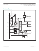


MAX16952
Maxim Integrated | 20www.maximintegrated.com
36V, 2.2MHz Step-Down Controller
with Low Operating Current
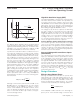
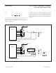
by the inductor and output capacitor, resulting in a
smaller phase shift and requiring less elaborate error-
amplifier compensation than voltage-mode control. A
simple single-series resistor (R
C
) and capacitor (C
C
)
are required to have a stable, high-bandwidth loop in
applications where ceramic capacitors are used for
output filtering (Figure 5). For other types of capacitors,
due to the higher capacitance and ESR, the frequency
of the zero created by the capacitance and ESR is
lower than the desired closed-loop crossover frequen-
cy. To stabilize a nonceramic output capacitor loop,
add another compensation capacitor (C
F
) from COMP
to SGND to cancel this ESR zero.
The basic regulator loop is modeled as a power modu-
lator, output feedback divider, and an error amplifier.
The power modulator has a DC gain set by g
mc
×
R
LOAD
, with a pole and zero pair set by R
LOAD
, the out-
put capacitor (C
OUT
), and its ESR. The following equa-
tions determine the approximate value for the gain of
the power modulator (GAIN
MOD(dc)
), neglecting the
effect of the ramp stabilization. Ramp stabilization is
necessary when the duty cycle is above 50% and is
internally and automatically done for the MAX16952:
where R
LOAD
= V
OUT
/I
OUT(MAX)
in Ω, f
SW
is the switch-
ing frequency in MHz, L is the output inductance in μH,
and g
mc
= 1/(A
V_CS
× R
DC
) in S. A
V_CS
is the voltage
gain of the current-sense amplifier and is typically
11V/V. R
DC
is the DC-resistance of the inductor or the
current-sense resistor in Ω.
In a current-mode step-down converter, the output
capacitor, its ESR, and the load resistance introduce a
pole at the following frequency:
The output capacitor and its ESR also introduce a zero at:
When C
OUT
is composed of n identical capacitors in
parallel, the resulting C
OUT
= n × C
OUT(EACH)
, and ESR
= ESR
(EACH)
/n. Note that the capacitor zero for a paral-
lel combination of like capacitors is the same as for an
individual capacitor.
The feedback voltage-divider has a gain of GAIN
FB
=
V
FB
/V
OUT
, where V
FB
is 1V (typ).
The transconductance error amplifier has a DC gain of
GAIN
EA(dc)
= g
m,EA
× R
OUT,EA
, where g
m,EA
is the
error amplifier transconductance, and R
OUT,EA
is the
output resistance of the error amplifier. Use g
m,EA
of
2500μS (max) and R
OUT,EA
of 30MΩ (typ) for compen-
sation design with the highest phase margin.
A dominant pole (f
dpEA
) is set by the compensation
capacitor (C
C
), the compensation resistor (R
C
), and the
amplifier output resistance (R
OUT,EA
). A zero (f
zEA
) is
set by the compensation resistor (R
C
) and the compen-
sation capacitor (C
C
). There is an optional pole (f
pEA
)
set by C
F
and R
C
to cancel the output capacitor ESR
zero if it occurs near the crossover frequency (f
C
,
where the loop gain equals 1 (0dB)).
Thus:
The loop-gain crossover frequency (f
C
) should be set
below 1/5 the switching frequency and much higher
than the power-modulator pole (f
pMOD
):
The total loop gain as the product of the modulator
gain, the feedback voltage-divider gain, and the error
amplifier gain at f
C
should be equal to 1. So:
For the case where f
zMOD
is greater than f
C
:
GAIN g R
GAIN GAIN
EA fC
mEA C
MOD fC
MOD dc
()
()
=×
=×
,
()
ff
f
pMOD
C
GAIN
V
V
GAIN
MOD fC
FB
OUT
EA fC
() ()
×× =1
ff
f
pMOD C
SW
<< ≤
5
f
CR R
f
CR
f
dpEA
COUTEAC
zEA
CC
pEA
=
×× +
()
=
××
1
2
1
2
π
π
,
==
××
1
2π CR
FC
f
ESR C
zMOD
OUT
=
××
1
2π
f
C
RfL
RfL
ESR
pMOD
OUT
LOAD SW
LOAD SW
=
××
××
+×
()
+
1
2π
⎛⎛
⎝
⎜
⎜
⎞
⎠
⎟
⎟
GAIN g
RfL
RfL
MOD dc mc
LOAD SW
LOAD SW
()
≅×
××
+×
()