
Datasheet


Maxim Integrated | 15www.maximintegrated.com
MAX16952
36V, 2.2MHz Step-Down Controller
with Low Operating Current
The adaptive driver dead-time allows operation without
shoot-through with a wide range of MOSFETs, minimiz-
ing delays and maintaining efficiency. To minimize stray
impedance, use very short, wide traces (50 mils to 100
mils wide if the MOSFET is 1in from the controller).
Synchronous rectification reduces conduction losses in
the rectifier by replacing the normal low-side Schottky
catch diode with a low-resistance MOSFET switch. The
internal pulldown transistor that drives DL low is robust,
with a 2Ω (typ) on-resistance. This low on-resistance
helps prevent DL from being pulled up during the fast
rise time of the LX node, due to capacitive coupling
from the drain to the gate of the low-side synchronous
rectifier MOSFET. Applications with high-input voltages
and long-inductive driver traces can require additional
gate-to-source capacitance. This ensures that fast-ris-
ing LX edges do not pull up the low-side MOSFET’s
gate, causing shoot-through currents. The capacitive
coupling between LX and DL created by the MOSFET’s
gate-to-drain capacitance (C
GD
= C
RSS
), gate-to-
source capacitance (C
GS
= C
ISS
- C
GD
), and additional
board parasitic should not exceed the following mini-
mum threshold:
Although a low-resistive path from DH and DL to the
MOSFET gates is encouraged, there are cases where
series resistors can be added. For instance, a series
resistor can be added to the DL path. However, in this
case, the design should have at least as much resis-
tance in series with the BST cap in order to help pre-
vent shootthrough current.
High-Side Gate-Drive Supply (BST)
The high-side MOSFET is turned on by closing an inter-
nal switch between BST and DH. This provides the
necessary g ate-to-source voltage to turn on the high-
side MOSFET, an action that boosts the gate-drive signal
above V
SUP
. The boost capacitor connected between
BST and LX holds up the voltage across the flying gate
driver during the high-side MOSFET on-time.
The charge lost by the boost capacitor for delivering
the gate charge is refreshed when the high-side
MOSFET is turned off and the LX node swings down
to ground. When the LX node is low, an internal high-
voltage switch connected between BIAS and BST
recharges the boost capacitor to the BIAS voltage.
See the
Boost-Flying Capacitor Selection
section to
choose the right size of the boost capacitor.
Dropout Behavior During Undervoltage Transients
The controller generates a low-side pulse every eight
clock cycles to refresh the BST capacitor during low-
dropout operation. This guarantees that the MAX16952
operates in dropout mode during undervoltage tran-
sients like cold crank. See the
Boost-Flying Capacitor
Selection
section for more details.
Current Limiting and Current-Sense Inputs
(CS and OUT)
The current-limit circuit uses differential current-sense
inputs (CS and OUT) to limit the peak inductor current.
If the magnitude of the current-sense signal exceeds
the current-limit threshold, the PWM controller turns off
the high-side MOSFET. The actual maximum load cur-
rent is less than the peak current-limit threshold by an
amount equal to half the inductor ripple current.
Therefore, the maximum load capability is a function of
the current-sense resistance, inductor value, switching
frequency, and duty cycle (V
OUT
/V
SUP
). See the
Current Sensing
section.
Design Procedure
Effective Input Voltage Range
Although the MAX16952 controller can operate from
input supplies up to 42V and regulate down to 1V, the
minimum voltage conversion ratio (V
OUT
/V
SUP
) might
be limited by the minimum controllable on-time. For
proper fixed-frequency PWM operation, the voltage
conversion ratio should obey the following condition:
where t
ON(MIN)
is 80ns and f
SW
is the switching fre-
quency in Hz. If the desired voltage conversion does
V
V
tf
OUT
SUP
ON MIN SW
>×
()
VV
C
C
GS TH SUP
RSS
ISS
()
>
⎛
⎝
⎜
⎞
⎠
⎟
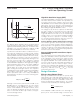
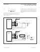
Figure 1. Pulse-Skipping/Discontinuous Crossover Point
INDUCTOR CURRENT
TIME
0
V
OUT
V
SUP
f
SW
t
ON(SKIP)
=
ON-TIME
I
PK
I
LOAD
= I
PK
/2