
Datasheet


MAX16952
Maxim Integrated | 14www.maximintegrated.com
36V, 2.2MHz Step-Down Controller
with Low Operating Current
exceeds the required load current and discharges
when the inductor current is lower, smoothing the volt-
age across the load. Under soft-overload conditions,
when the peak inductor current exceeds the selected
current limit, the high-side MOSFET is turned off imme-
diately. The low-side MOSFET is turned on and
remains on to let the inductor current ramp down until
the next clock cycle.
Forced Fixed-Frequency PWM Mode
The low-noise forced fixed-frequency PWM mode
(FSYNC connected to BIAS or an external clock) dis-
ables the zero-crossing comparator, which controls the
low-side switch on-time. This forces the low-side gate-
driver waveform to constantly be the complement of the
high-side gate-drive waveform. The inductor current
reverses at light loads while DH maintains a duty factor
of V
OUT
/V
SUP
.
The benefit of forced fixed-frequency PWM mode is to
keep the switching frequency fairly constant. However,
forced fixed-frequency PWM operation comes at a cost:
the no-load 5V supply current can be up to 45mA,
depending on the external MOSFETs and switching fre-
quency. Forced fixed-frequency PWM mode is most
useful for avoiding audio frequency noises and improv-
ing load-transient response.
Light-Load Low-Quiescent Operating
(Skip) Mode
The MAX16952 includes a light-load operating mode
control input (FSYNC = SGND) used to enable or dis-
able the zero-crossing comparator. When the zero-
crossing comparator is enabled, the regulator forces
DL low when the current-sense inputs detect zero
inductor current. This keeps the inductor from discharg-
ing the output capacitor and forces the regulator to skip
pulses under light-load conditions to avoid overcharg-
ing the output.
The lowest operating currents can be achieved in skip
mode. When the MAX16952 operates in skip mode with
no external load current, the overall current consump-
tion can be as low as 50μA. A disadvantage of skip
mode is that the operating frequency is not fixed.
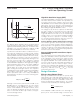
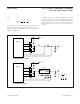
Skip-Mode Current-Sense Threshold
When skip mode is enabled, the on-time of the step-
down controller terminates when the output voltage
exceeds the feedback threshold and when the current-
sense voltage exceeds the idle-mode current-sense
threshold (V
CS,IDLE
). See Figure 1. Under light-load
conditions, the on-time duration depends solely on the
skip-mode current-sense threshold, which is 25mV (typ).
This forces the controller to source a minimum amount
of power with each cycle. To avoid overcharging the
output, another on-time cannot begin until the output
voltage drops below the feedback threshold. Because
the zero-crossing comparator prevents the switching
regulator from sinking current, the controller must skip
pulses. Therefore, the controller regulates the valley of
the output ripple under light-load conditions.
Automatic Pulse-Skipping Crossover
In skip mode, an inherent automatic switchover to pulse
frequency modulation (PFM) takes place at light loads.
This switchover is affected by a comparator that trun-
cates the low-side switch on-time at the inductor cur-
rent’s zero crossing. The zero-crossing comparator
senses the inductor current across CS to OUT. Once
(V
CS
- V
OUT
) drops below the 6mV zero-crossing, cur-
rent-sense threshold, the comparator forces DL low.
This mechanism causes the threshold between pulse-
skipping PFM and nonskipping PWM operation to coin-
cide with the boundary between continuous and
discontinuous inductor-current operation (also known
as the critical conduction point). The load-current level
at which PFM/PWM crossover occurs, I
LOAD(SKIP)
, is
given by:
The switching waveforms can appear noisy and asyn-
chronous when light-loading causes pulse-skipping
operation. This is a normal operating condition that
results in high light-load efficiency. Trade-offs in PFM
noise vs. light-load efficiency is made by varying the
inductor value. Generally, low inductor values pro-
duce higher efficiency under light load, while higher
values result in higher full-load efficiency (assuming
that the coil resistance remains constant) and less
output-voltage ripple. Drawbacks of using higher
inductor values include larger physical size and
degraded load-transient response (especially at low
input-voltage levels).
MOSFET Gate Drivers (DH and DL)
The DH and DL drivers are optimized for driving logic-
level n-channel power MOSFETs. The DH high-side n-
channel MOSFET driver is powered by charge pumping
at BST, while the DL synchronous rectifier drivers are
powered directly by the 5V linear regulator (BIAS).
An adaptive dead-time circuit monitors the DH and DL
outputs and prevents the opposite-side MOSFET from
turning on until the other MOSFET is fully off. Thus, the
circuit allows the high-side driver to turn on only when
the DL gate driver has been turned off. Similarly, it pre-
vents the low-side (DL) from turning on until the DH
gate driver has been turned off.
IA
VVV
VfMHz
LOAD SKIP
SUP OUT OUT
SUP SW
()
[]
=
−
()
××2
[[]
×
[]
LμH