
Datasheet


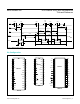


PIN
NAME FUNCTIONMAX155 MAX156
PDIP/SO PDIP SO
1 23 26 AIN3 Sampling Analog Input, Channel 3
2 24 28 AIN2 Sampling Analog Input, Channel 2
3 1 2 AIN1 Sampling Analog Input, Channel 1
4 2 4 AIN0 Sampling Analog Input, Channel 0
5 3 5 MODE Mode congures multiplexer and converter. See Table 4.
6 4 6 V
SS
Negative Supply. Power V
SS
with -5V for extended input range.
7 5 7 CS CHIP SELECT Input must be low for the ADC to recognize RD, or WR
8 6 8 RD READ Input reads data sequentially from RAM
9 7 9 WR
WRITE Input’s rising edge initiates conversion and updates channel conguration
register. Falling edge samples inputs.
10 8 10 BUSY BUSY Output low when conversion is in progress
11 9 11 CLK External Clock Input
12 10 12 D7/ALL Three-State Data Output Bit 7 (MSB)/Sequential or Specic Conversion
13 11 13 D6/DIFF Three-State Data Output Bit 6/Single-Ended/Differential Select
14 12 14 DGND Digital Ground
15 13 15 D5/BIP Three-State Data Output Bit 5/Unipolar/Bipolar Conversion
16 14 16 D4/INH Three-State Data Output Bit 4/Inhibit Conversion Input
17 15 17 D3/PD Three-State Data Output Bit 3/Power-Down Input
18 16 18 D2/A2 Three-State Data Output Bit 2/RAM Address Bit A2 (MAX155 Only)
19 17 19 D1/A1 Three-State Data Output Bit 1/RAM Address Bit A1
20 18 20 D0/A0 Three-State Data Output Bit 0/RAM Address Bit A0
21 19 21 REFOUT Reference Output, +2.5V
22 20 22 REFIN Reference Input, +2.5 Normally
23 21 23 AGND Analog Ground
24 22 24 V
DD
Power-Supply Voltage, +5V Normally
25–28 — — AIN7–4 Sampling Analog Input, Channels 7–4
— —
1, 3,
25, 27
N.C. No Connection. No internal connection—pin unconnected.
MAX155/MAX156 8-/4-Channel ADCs with Simultaneous
T/Hs and Reference
www.maximintegrated.com
Maxim Integrated
│
7
Pin Description