
Datasheet
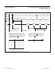
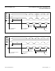

For this example, 6 write operations (with each
address and data setting in Table 5 above) load the
mux after power-up.
2) Sample all selected channels with a WR pulse (and
INH = 0), and update or rewrite any one location of
the configuration register.
This write operation may be skipped by loading INH with a
0 on the last WR of the above step. The conversion then
starts on the 6th WR. DIFF and SIP cannot be changed
on the 6th WR in the conversion is started at that time.
When the conversion starts, BUSY goes low while all
selected channels are sequentially converted. Conversion
results are stored in RAM and are ready to read when
BUSY returns high.
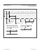
3) Data is read from RAM with INH = L and consecutive
RD strobes. Note that in the 6 channel configurations
described in this example (Figure 10), 6 RD pulses
access all available data, start with the differential
channel (1, 0). Additional RD pulses loop around,
accessing the lowest chan nel data again.
4) To start a new conversion cycle with the same mux
configuration, repeat steps 2 and 3.
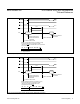
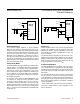
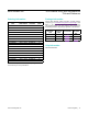
Figure 10. MAX155/MAX156 Typical Operating Circuit
MAX155
AIN
(1)
DIFFERENTIAL
BIPOLAR
(0)
(2) BIPOLAR
(-) 3
(+) 4
REFIN
REFOUT
22
21
2
(3) BIPOLAR
1
DIFFERENTIAL
UNIPOLAR
(4) BIPOLAR
28
(5) BIPOLAR
(6)
(7)
27
2.5V
-1.75V
AGND
23 14 6
DGND V
SS
(+) 26
(-) 25
SENSOR
47µF
-5V
0.1µF
47µF0.1µF
V
DD
+5V
+24
47µF0.1µF
CLK CLOCK
11
MODE
5
CS
7
RD
8
WR
9
BUSY
10
20...15, 13, 12
D0–D7 DATA I/0 LINES
8
MAX155/MAX156 8-/4-Channel ADCs with Simultaneous
T/Hs and Reference
www.maximintegrated.com
Maxim Integrated
│
18