
Datasheet

Conversion Time
Conversion time is calculated by:
t
CONV
= (9 x N x 2)/f
CLK
where N is the number of channels converted. This
includes one clock cycle of uncertainty. For a single
channel and 5MHz clock, the conversion time is (9 x 1 x
2)/5MHz = 3.6µs. For the MAX155, the maxi mum conver-
sion time for 8 channels is (9 x 8 x 2)/5MHz = 28.8µs. In
the application example (Figure 10), six conversions are
configured, and the conversion time is (9 x 6 x 2}/5MHz
= 21.6µs.
Applications Information
9-Bit A/D Conversion
In I/O mode, a 9th bit of resolution can be created by per-
forming two unipolar differential conversions with opposite
input polarities (i.e., first with AIN0[+] and AIN1[-], then with
AINO[-] and AIN1[+]). Only the A0 bit must be changed to
reverse input channel polarity (Table 3). The sign reversal
also occurs on the current write without a one conversion
delay. For a differential input signal, one of the two conver-
sions will read 0 while the other will contain an 8-bit result.
The input polarity that provides the 8-bit result indicates
the 9th (sign) bit. 4 channels can be measured this way. A
major drawback of this technique is that many of the sam-
pling features of the MAX155/MAX156 are defeated since
two separate samples are needed
If only two 9-bit channels are needed, then two separate
differential channels with reversed input polarities can be
connected so that both input pairs sample at the same
time. This way the simultaneoussampling advantages of
the MAX155/MAX156 are retained.
Typical I/O Mode Application
The MAX155/MAX156 address and configuration inputs
for this example were determined by selecting the desired
channel configurations in Tables 2 and 3. Figure 10 illus-
trates the configuration outlined in Table 5.
An A/D conversion in I/O mode involves the following
steps:
1) Configure the mux by loading data into the con-
figuration register based on selections from Table 2
and/or 3 (with INH = 1 and MODE = open circuit).
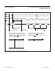
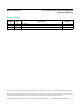
Figure 9a. Transfer Function—Unipolar Operation
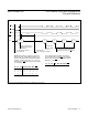
Figure 9b. Transfer Function—Bipolar Operation
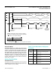
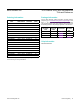
Table 5. Typical Multiplexer Configuration
A2 A1 A0 DIFF BIP FUNCTION
0 0 1 1 1
Channel (1, 0) Differential
Bipolar
0 1 0 0 0
Channel 2 Single-Ended,
Unipolar
0 1 1 0 1
Channel 3 Single-Ended,
Bipolar
1 0 0 0 1
Channel 4 Single-Ended,
Bipolar
1 0 1 0 0
Channel 5 Single-Ended,
Unipolar
1 1 0 1 0
Channel (6. 7)
Differential, Unipolar
OUTPUT
CODE
(FS - 3/2 LSB)
FS = V
REF
FS
256
1 LSB =
1111 1111
1111 1110
1111 1101
0000 0011
0000 0010
0000 0001
0000 0000
0 1 LSB
2 LSBs
AIN, INPUT VOLTAGE (LSB)
FS - 1 LSB FS
AIN
3 LSBs
OUTPUT
CODE
FS = 2V
REF
FS
256
1 LSB =
0111 1111
0111 1110
0000 0010
0000 0001
1111 1111
1111 1110
1000 0001
1000 0000
0000 0000
+FS - 1 LSB
AIN
-1/2 LSB
+1/2 LSB
MAX155/MAX156 8-/4-Channel ADCs with Simultaneous
T/Hs and Reference
www.maximintegrated.com
Maxim Integrated
│
17