
Datasheet

Extemal Reference
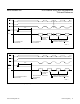
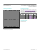
If an external voltage reference is used at REFIN,
REFOUT must either be bypassed (Figure 8b) or dis-
abled to prevent its output from oscillating and generating
unwanted conversion noise elsewhere in the ADC. If com-
ponent count is critical when using an external reference,
REFOUT may be disabled by connecting it to V
DD
. In
this case, the unused internal reference does not need a
bypass cap. A disadvantage of tying REFOUT to V
DD
is
that power-down current will be increased by about 250µA
above the specification limits.
Power-Down Mode
The MAX155/MAX156 may be placed in a powered-down
state by writing a 1 to the PD location in the configuration
register (Table 1). The register may be updated while in
this state (to change mux configurations or exit power-
down mode) and all register contents are retained; how-
ever no data can be read from RAM and no conversions
can be started. The power-down command is implement-
ed on WR’s rising edge.
To minimize current drain, the MAX155/MAX156 inter-
nal reference is turned off during power-down. When
returning to normal operation (PD = 0), up to 5ms may
be needed to allow the reference to recharge its 4.7µF
bypass capacitor before a conversion is performed. If an
external reference is used, and remains on during power-
down, a conversion can be started within 50µs after load-
ing PD with a 0.
Bypassing
A 47µF electrolytic and a 0.1µF ceramic capacitor should
bypass V
DD
to AGND. If input signals below ground are
expected, a negative supply is necessary. In that case,
V
SS
should be bypassed to AGND with a 4.7µF and
0.1µF combination.
The internal reference requires a 4.7µF and 0.1µF com-
bination. If an external voltage reference is used, bypass
REFIN to AGND with a 4.7µF capacitor close to the chip.
When an external reference is used, REFOUT must still
be either bypassed or connected to V
DD
.
Track/Hold Ampliers
The MAX155/MAX156 T/H amplifiers’ high input imped-
ance usually requires no input buffering. All T/Hs sample
simultaneously. For best results, the analog inputs should
not exceed the power-supply rails (V
DD
, V
SS
) by more
than 50mV.
The time required for the T/H to acquire an input signal
for one channel is a function of how quickly the channel
input capacitance is charged. If the source impedance of
the input signal is high, acquisition takes longer, and more
time must be allowed between conversions. Acquisition
time is calculated by:
t
ACQ
= 8(R
S
+ R
IN
) x 4pF (but never less than 800ns)
where R
IN
= 15kΩ, and R
S
= source impedance of the
ADC’s input signal.
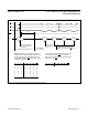
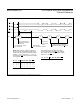
Figure 8a. Internal Reference Figure 8b. External Reference, +2.5V Full Scale
AINx
REFOUT
REFIN
AGND
V
SS
V
DD
AINx (+)
AINx (-)
0.1µF4.7µF
0.1µF47µF
+5V
MAX155
MAX156
AINx
REFIN
AGND
V
SS
REFOUT
V
DD
AINx (+)
AINx (-)
0.1µF
+2.5V
4.7µF
0.1µF47µF
+5V
MAX155
MAX156
MAX584
4.7µF
MAX155/MAX156 8-/4-Channel ADCs with Simultaneous
T/Hs and Reference
www.maximintegrated.com
Maxim Integrated
│
16