
Datasheet
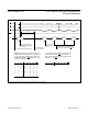
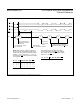
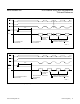
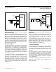
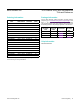
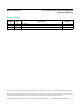

Figure 5a. Input/Output Mode Timing–Single-Channel, Single-Ended Conversion
Figure 5b. Input/Output Mode Timing–Single-Channel, Differential Conversion
t
CONV
CS
WR
RD
BUSY
D0-D7
DATA IN DATA OUT
UPDATE CONFIGURATION
REGISTER AND BEGIN NEW
CONVERSION
CHANNEL IS SAMPLED HERE
NOTE: A single-ended channel is converted by writing
the following data into the configuration register
(see Figure 3) The BIP and DIFF bits are not implemented
until the next WR
S = May be selected
A0 A1 A2 PD INH BIP DIFF ALL
S S S 0 0 S 0 1
END OF CONVERSION
READ DATA INDICATED
BY ADDRESS
t
CONV
CS
WR
RD
BUSY
D0-D7
DATA IN DATA OUT
UPDATE CONFIGURATION
REGISTER AND BEGIN NEW
CONVERSION
CHANNEL IS SAMPLED HERE
NOTE: A differential channel is converted by writing
the following data into the configuration register
(see Figure 3) The BIP and DIFF bits are not
implemented until the next WR
S = May be selected
A0 A1 A2 PD INH BIP DIFF ALL
S S S 0 0 S 1 1
END OF CONVERSION
READ DATA INDICATED
BY ADDRESS
MAX155/MAX156 8-/4-Channel ADCs with Simultaneous
T/Hs and Reference
www.maximintegrated.com
Maxim Integrated
│
13