
Datasheet
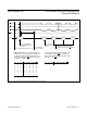
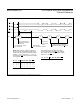
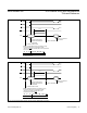
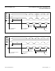
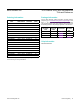
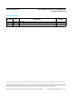

Figure 4b. Input/Output Mode Timing–Four Differential Conversions
t
CONV
DATA IN
CONVERSION END
OF ALL 4 DIFFERENTIAL CHANNELS
ACCESSED BY CONSECUTIVE RD PULSES
CONSECUTIVE RAM LOCATIONS ARE
UPDATE CONFIGURATION
REGISTER AND BEGIN NEW
CONVERSION
0,1 2,3 4,5 6,7
THE FIRST RAM
LOCATION READ
IS CH 0,1
CS
WR
RD
BUSY
D0-D7
A0 A1 A2 PD INH BIP DIFF ALL
0 0 0 0 1 S 0 0
1 1 0 0 1 S 0 0
0 0 1 0 1 S 0 0
1 1 1 0 1 S 0 0
Once the above data is loaded, all channels
are converted with a single WR to any address
(this is where the above timing diagram begins).
With INH = 0, and ALL = 0:
S = May be selected
A0 A1 A2 PD INH BIP DIFF ALL
0 0 0 0 0 S 0 0
NOTE: After power-up, and prior to the above
timing sequence, all differential channels must
be set up by writing to the configuration register.
(AIN0, 2, 4, 6 are +, and AIN1, 3, 5, 7 are - for
this example). 4 WRs (see Figure 3) are needed
for 8 channels:
ALL 4 DIFFERENTIAL CHANNELS
ARE SAMPLED HERE
MAX155/MAX156 8-/4-Channel ADCs with Simultaneous
T/Hs and Reference
www.maximintegrated.com
Maxim Integrated
│
12