
Datasheet


High-Efficiency, 3A, Current-Mode
Synchronous, Step-Down Switching Regulator
MAX15058
______________________________________________________________________________________ 15
t
OFF1
is the time needed for inductor current to reach the
zero-current crossing limit (~0A):
SKIP LIMIT
OFF1
OUT
L I
t
V
−
×
=
During t
ON
and t
OFF1
, the output capacitor stores a
charge equal to (see Figure 2):
( )
2
SKIP LIMIT LOAD
IN OUT OUT
OUT
1 1
L x I I x
V V V
Q
2
−
− +
−
∆ =
During t
OFF2
(= n x t
CK
, number of clock cycles skipped),
output capacitor loses this charge:
( )
OUT
OFF2
LOAD
2
SKIP LIMIT LOAD
IN OUT OUT
OFF2
LOAD
Q
t
I
1 1
L x I I x
V V V
t
2 xI
−
∆
= ⇒
− +
−
=
Finally, frequency in skip mode is:
SKIP
ON OFF1 OFF2
1
f
t t t
=
+ +
Output ripple in skip mode is:
( )
( )
( )
( )
OUT RIPPLE COUT RIPPLE ESR RIPPLE
SKIP LIMIT LOAD ON
OUT
ESR,COUT SKIP LIMIT LOAD
SKIP LIMIT
OUT RIPPLE ESR,COUT
OUT IN OUT
SKIP LIMIT LOAD
V V V
I I x t
C
R x I I
L x I
V R
C x V V
x I I
− − −
−
−
−
−
−
= +
−
=
+ −
= +
−
−
To limit output ripple in skip mode, size C
OUT
based on
the above formula. All the above calculations are appli-
cable only in skip mode.
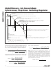
Compensation Design Guidelines
The MAX15058 uses a fixed-frequency, peak-current-mode
control scheme to provide easy compensation and fast
transient response. The inductor peak current is monitored
on a cycle-by-cycle basis and compared to the COMP
voltage (output of the voltage error amplifier). The regula-
tor’s duty cycle is modulated based on the inductor’s peak
current value. This cycle-by-cycle control of the inductor
current emulates a controlled current source. As a result,
the inductor’s pole frequency is shifted beyond the gain
bandwidth of the regulator. System stability is provided
with the addition of a simple series capacitor-resistor from
COMP to GND. This pole-zero combination serves to tailor
the desired response of the closed-loop system. The basic
regulator loop consists of a power modulator (comprising
the regulator’s pulse-width modulator, current sense and
slope compensation ramps, control circuitry, MOSFETs,
and inductor), the capacitive output filter and load, an
output feedback divider, and a voltage-loop error amplifier
with its associated compensation circuitry. See Figure 1.
The average current through the inductor is expressed as:
L MOD COMP
I G V= ×
where IL is the average inductor current and G
MOD
is the
power modulator’s transconductance.
For a buck converter:
OUT LOAD L
V R I= ×
where R
LOAD
is the equivalent load resistor value.
Combining the above two relationships, the power mod-
ulator’s transfer function in terms of VOUT with respect
to VCOMP is:
OUT LOAD L
LOAD MOD
COMP L
MOD
V R I
R G
V I
G
×
= = ×
The peak current-mode controller’s modulator gain
is attenuated by the equivalent divider ratio of the
load resistance and the current-loop gain’s impedance.
G
MOD
becomes:
( )
( )
MOD MC
LOAD
S
SW
1
G DC g
R
1 K 1 D 0.5
f L
= ×
+ × × − −
×
where R
LOAD
= V
OUT/IOUT(MAX)
, f
SW
is the switching
frequency, L is the output inductance, D is the duty cycle
(V
OUT
/V
IN
), and K
S
is a slope compensation factor cal-
culated from the following equation:
( )
SLOPE SLOPE SW MC
S
N IN OUT
S V f L g
K 1 1
S V V
× × ×
= + = +
−
where:
SLOPE
SLOPE SLOPE SW
SW
V
S V f
t
= = ×
( )
IN OUT
N
MC
V V
S
L g
−
=
×