
Datasheet

Output Driver
The MAX15018_/MAX15019_ drivers contain low on-
resistance p-channel and n-channel devices in a totem
pole configuration for the driver output stage. This
allows for rapid turn-on and turn-off of high gate-charge
(Q
g
) external switching MOSFETs.
The drivers exhibit low drain-to-source resistance
(R
DS_ON
), which decreases for higher values of V
DD
and for lower operating temperatures. Lower R
DS_ON
means higher source and sink currents from the IC,
and results in faster switching speeds, since the exter-
nal MOSFET gate capacitance will charge and dis-
charge at a quicker rate. The peak source and sink
current provided by the drivers is typically 3A.
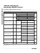
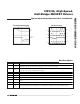
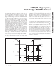
Propagation delay from the logic inputs to the driver
outputs is matched to within 8ns (max) between the
low-side and high-side drivers. Turn-on and turn-off
propagation delays are typically 35ns and 36ns. See
Figure 1. The internal drivers also contain break-before-
make logic to eliminate shoot-through conditions that
would cause unnecessarily high operating supply cur-
rents, efficiency reduction, and voltage spikes at V
DD
.
Voltage at DL is approximately equal to V
DD
when in a
high state, and zero when in a low state. Voltage from
DH to HS is approximately equal to V
DD
minus the
diode drop of the integrated bootstrap diode when in a
high state, and zero when in a low state. The high-side
MOSFET’s continuous on-time is limited due to the
charge loss from the high-side driver’s quiescent cur-
rent. The maximum on-time is dependent on the size of
the bootstrap capacitor (C
BST
), I
BST
(190µA max), and
V
BST_UVLO
.
Integrated Bootstrap Diode
An integrated diode between V
DD
and BST is used in
conjunction with an external bootstrap capacitor (C
BST
)
to provide the voltage required to turn on the high-side
MOSFET (see the
Typical Operating Circuit
). The inter-
nal diode charges the bootstrap capacitor from V
DD
when the low-side switch is on, and isolates V
DD
when
HS is pulled high when the high-side driver turns on.
The internal bootstrap diode has a typical forward volt-
age drop of 0.9V and has a 40ns (typ) turn-off/-on time.
The turn-off time (reverse recovery time) depends on
the reverse-recovery current and can be as low as
10ns. If a lower diode voltage-drop between V
DD
and
BST is needed, connect an external Schottky diode
between V
DD
and BST.
MAX15018/MAX15019
125V/3A, High-Speed,
Half-Bridge MOSFET Drivers
_______________________________________________________________________________________ 9
Figure 1. Timing Characteristics of Logic Inputs (MAX15018A/MAX15019A)
IN_L
DL
t
D_OFF1
IN_H
V
IL
V
IL
DH
90%
10%
90%
10%
V
IH
V
IH
t
R
t
R
t
D_ON1
t
D_OFF1
t
MATCH
= (t
D_ON2
- t
D_ON1
) OR (t
D_OFF2
- t
D_OFF1
)
t
F
t
F
t
D_ON2