
Datasheet
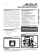
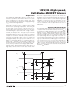

MAX15018/MAX15019
125V/3A, High-Speed,
Half-Bridge MOSFET Drivers
2 _______________________________________________________________________________________
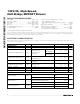
ABSOLUTE MAXIMUM RATINGS
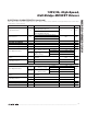
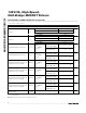
ELECTRICAL CHARACTERISTICS
(V
DD
= V
BST
= 8V to 12.6V, V
HS
= V
GND
= 0V, T
A
= T
J
= -40°C to +125°C, unless otherwise noted. Typical values are at V
DD
= V
BST
= 12V and T
A
= +25°C.) (Note 1)
Stresses beyond those listed under “Absolute Maximum Ratings” may cause permanent damage to the device. These are stress ratings only, and functional
operation of the device at these or any other conditions beyond those indicated in the operational sections of the specifications is not implied. Exposure to
absolute maximum rating conditions for extended periods may affect device reliability.
V
DD
to GND............................................................-0.3V to +15V
IN_H, IN_L to GND .................................................-0.3V to +15V
DL to GND..................................................-0.3V to (V
DD
+ 0.3V)
DH to HS.....................................................-0.3V to (V
DD
+ 0.3V)
BST to HS ...............................................................-0.3V to +15V
HS to GND (repetitive transient)..............................-5V to +130V
HS dv/dt to GND................................................................50V/ns
Continuous Power Dissipation (T
A
= +70°C)
Single and Multilayer Board
8-Pin SO-EP (derate 23.8mW/°C above +70°C)*..........1.904W
θ
JC
...................................................................................6°C/W
Operating Temperature .....................................-40°C to +125°C
Maximum Junction Temperature .....................................+150°C
Storage Temperature Range .............................-65°C to +150°C
Lead Temperature (soldering, 10s) .................................+300°C
PARAMETER SYMBOL CONDITIONS MIN TYP MAX UNITS
POWER SUPPLY
Operating Supply Voltage V
VDD
8.0 12.6 V
MAX15018A/
MAX15018B
65 130
V
DD
Quiescent Supply Current I
DDQ
IN_H and IN_L are
unconnected (no
switching)
MAX15019A/
MAX15019B
95 190
µA
V
DD
Operating Supply Current I
DDO
f
SW
= 500kHz, V
DD
= 12V,
no capacitive load
2.75 3.75 mA
BST Quiescent Supply Current I
BSTQ
IN_H and IN_L are unconnected (no
switching)
95 190 µA
BST Operating Supply Current I
BSTO
f
SW
= 500kHz, V
BST
- V
HS
= 12V, no
capacitive load
2.75 3.75 mA
UVLO (V
DD
to GND) V
DD_UVLO
V
DD
rising 6.5 7.3 8 V
UVLO (BST to HS) V
BST_UVLO
V
BST
rising 6.2 6.9 7.6 V
UVLO Hysteresis 0.5 V
LOGIC INPUT
MAX15018A/MAX15018B (CMOS)
0.67 x
V
DDInput-Logic High V
IH
MAX15019A/MAX15019B (TTL) 2
V
MAX15018A/MAX15018B (CMOS)
0.33 x
V
DD
Input-Logic Low V
IL
MAX15019A/MAX15019B (TTL) 0.8
V
MAX15018A/MAX15018B (CMOS) 1.65
Logic-Input Hysteresis V
HYS
MAX15019A/MAX15019B (TTL) 0.4
V
*
As per JEDEC Standard 51 (Single-Layer Board).