
Datasheet
MAX15012/MAX15013
175V/2A, High-Speed,
Half-Bridge MOSFET Drivers
2 _______________________________________________________________________________________
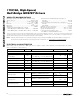
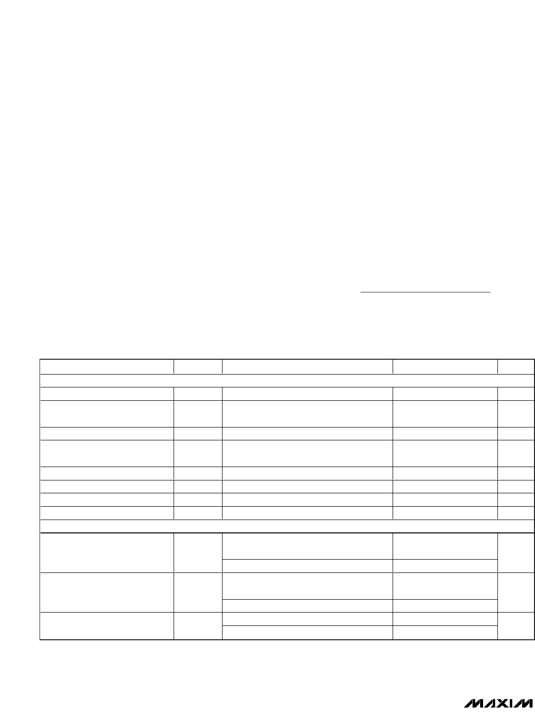
ABSOLUTE MAXIMUM RATINGS
ELECTRICAL CHARACTERISTICS
(V
DD
= V
BST
= +8V to +12.6V, V
HS
= GND = 0V, T
A
= T
J
= -40°C to +125°C, unless otherwise noted. Typical values are at V
DD
=
V
BST
= +12V and T
A
= +25°C.) (Note 2)
Stresses beyond those listed under “Absolute Maximum Ratings” may cause permanent damage to the device. These are stress ratings only, and functional
operation of the device at these or any other conditions beyond those indicated in the operational sections of the specifications is not implied. Exposure to
absolute maximum rating conditions for extended periods may affect device reliability.
(All voltages referenced to GND, unless otherwise noted.)
V
DD
, IN_H, IN_L......................................................-0.3V to +14V
DL...............................................................-0.3V to (V
DD
+ 0.3V)
HS............................................................................-5V to +180V
DH to HS.....................................................-0.3V to (V
DD
+ 0.3V)
BST to HS ...............................................................-0.3V to +14V
dV/dt at HS ........................................................................50V/ns
Continuous Power Dissipation (T
A
= +70°C)
8-Pin SO (derate 5.9mW/°C above +70°C)...............470.6mW
8-Pin SO-EP (derate 19.2mW/°C above +70°C) .....1538.5mW
Junction-to-Case Thermal Resistance (
θ
JC
)(Note 1)
8-Pin SO .......................................................................40°C/W
8-Pin SO-EP....................................................................6°C/W
Junction-to-Ambient Thermal Resistance (θ
JA
)(Note 1)
8-Pin SO .....................................................................170°C/W
8-Pin SO-EP..................................................................52°C/W
Maximum Junction Temperature .....................................+150°C
Operating Temperature Range .........................-40°C to +125°C
Storage Temperature Range .............................-65°C to +150°C
Lead Temperature (soldering, 10s) .................................+300°C
PARAMETER
SYMBOL
CONDITIONS
MIN TYP MAX
UNITS
POWER SUPPLIES
Operating Supply Voltage V
DD
(Notes 3 and 4) 8.0
12.6
V
V
DD
Quiescent Supply Current
(No Switching)
I
DD
IN_H = IN_L = GND (for A/C versions),
IN_H = GND, IN_L = V
DD
(for B/D versions)
70
140
µA
V
DD
Operating Supply Current I
DDO
f
SW
= 500kHz, V
DD
= +12V 3 mA
BST Quiescent Supply Current I
BST
IN_H = IN_L = GND (for A/C versions),
IN_H = GND, IN_L = V
DD
(for B/D versions)
15 40 µA
BST Operating Supply Current I
BSTO
f
SW
= 500kHz, V
DD
= V
BST
= +12V 3 mA
UVLO (V
DD
to GND)
UVLO
VDD
V
DD
rising 6.5 7.3 8.0 V
UVLO (BST to HS)
UVLO
BST
BST rising 6.0 6.9 7.8 V
UVLO Hysteresis 0.5 V
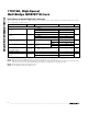
LOGIC INPUT
MAX15012_, CMOS (V
DD
/2) version
0.67 x
V
DD
0.55 x
V
DD
Input-Logic High V
IH_
MAX15013_, TTL version 2
1.65
V
MAX15012_, CMOS (V
DD
/2) version
0.4 x
V
DD
0.33 x
V
DD
Input-Logic Low V
IL_
MAX15013_, TTL version 1.4 0.8
V
MAX15012_, CMOS (V
DD
/2) version 1.6
Logic-Input Hysteresis V
HYS
MAX15013_, TTL version
0.25
V
*Per JEDEC 51 Standard Multilayer board.
Note 1: Package thermal resistances were obtained using the method described in JEDEC specification JE5D51-7, using a four-
layer board. For detailed information on package thermal considerations, see www.maxim-ic.com/thermal-tutorial
.