
Datasheet


Maxim Integrated
│
2
www.maximintegrated.com
MAX14970 Ruggedized 6Gbps SATA Redriver with High ESD
and Extended Temperature Operation
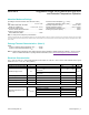
(All voltages referenced to GND, unless otherwise noted.)
V
CC
...................................................................... -0.3V to +4.0V
AINP, AINM, BINP, BINM, EN, CAD,
MODE, PA, PB (Note 1)
....................... -0.3V to (V
CC
+ 0.3V)
Short-Circuit Output Current
AOUTP, AOUTM, BOUTP, BOUTM
.............................. ±30mA
Continuous Current at Inputs
AINP, AINM, BINP, BINM
................................................ ±5mA
Continuous Power Dissipation (T
A
= +70ºC)
TQFN (derate 25.6mW/ºC above +70ºC)
................. 2051mW
Operating Temperature Range
........................... -40ºC to +85ºC
Storage Temperature Range
............................ -55ºC to +150ºC
Lead Temperature (soldering, 10s)
................................. +300ºC
Soldering Temperature (reflow)
....................................... +260ºC
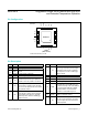
TQFN
Junction-to-Ambient Thermal Resistance (θ
JA
) .......... 39ºCW
Junction-to-Case Thermal Resistance (θ
JC
) ................ 6ºC/W
Absolute Maximum Ratings
Note 2: Package thermal resistances were obtained using the method described in JEDEC specification JESD51-7, using a four-layer
board. For detailed information on package thermal considerations, refer to www.maximintegrated.com/thermal-tutorial.
Note 1:
All I/O pins are clamped by internal diodes.
Stresses beyond those listed under “Absolute Maximum Ratings” may cause permanent damage to the device. These are stress ratings only, and functional operation of the device at these
or any other conditions beyond those indicated in the operational sections of the specifications is not implied. Exposure to absolute maximum rating conditions for extended periods may affect
device reliability.
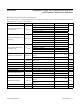
Package Thermal Characteristics (Note 2)
Electrical Characteristics
(V
CC
= +3.0V to +3.6V, C
CL
= 10nF coupling capacitor on each output, R
L
= 50Ω, T
A
= -40ºC to +85ºC, unless otherwise noted. Typical
values are at V
CC
= +3.3V, T
A
= +25ºC.) (Note 3)
PARAMETER SYMBOL CONDITIONS MIN TYP MAX UNITS
Operating Power-Supply Range V
CC
3.0 3.6 V
Operating Supply Current I
CC
PA = PB = V
CC
, D10.2 pattern, f = 3GHz,
active state
70 100
mA
PA = PB = GND, D10.2 pattern, f = 3GHz,
active state
60 85
Standby Supply Current I
STBY
EN = GND or CAD = V
CC
20 500 µA
Dynamic Power-Down Current I
DYNPD
16 20 mA
Differential Input Resistance Z
RX-DIFF-DC
(Note 4) 85 100 115 Ω
Differential Output Resistance Z
TX-DIFF-DC
(Note 4) 85 100 115 Ω
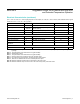
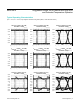
AC PERFORMANCE
Differential Input Return Loss
(Notes 4, 5)
RL
RX-DIFF
150MHz ≤ f < 300MHz 18
dB
300MHz ≤ f < 600MHz 14
600MHz ≤ f < 1200MHz 10
1.2GHz ≤ f < 2.4GHz 8
2.4GHz ≤ f ≤ 3.0GHz 3