
Datasheet


Maxim Integrated
│
10
www.maximintegrated.com
MAX14970 Ruggedized 6Gbps SATA Redriver with High ESD
and Extended Temperature Operation
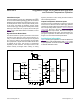
Exposed-Pad Package
The exposed-pad, 20-pin TQFN package incorporates
features that provide a very low-thermal resistance path
for heat removal from the device. The exposed pad on the
device must be soldered to GND for proper ther mal and
electrical performance. For more information on exposed-
pad packages, refer to Application Note 862: HFAN-08.1:
Thermal Considerations of QFN and Other Exposed-
Paddle Packages.
Layout
Use controlled-impedance transmission lines to interface
with the device’s high-speed inputs and outputs. Place
power-supply decoupling capacitors as close as possible
to the V
CC
pin.
Power-Supply Sequencing
Caution: Do not exceed the absolute maximum rat-
ings because stresses beyond the listed ratings can
cause permanent damage to the device.
Proper power-supply sequencing is recommended for all
devices. Always apply V
CC
before applying signals, espe-
cially if the signal is not current limited.
ESD Protection
As with all Maxim Integrated devices, ESD protection
structures are incorporated on all pins to protect against
electrostatic discharges encountered during handling and
assembly. The MAX14970 is protected against ESD events
up to Q
8kV (HBM). The ESD struc tures withstand Q8kV in
all states: normal operation and powered down. After an
ESD event, the device continues to function without latchup.
HBM
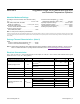
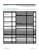
The device is rated for Q8kV ESD pro tection using the
HBM (MIL-STD-883, Method 3015). Figure 2 shows the
HBM voltage, and Figure 3 shows the current waveform it
generates when discharged into a low-impedance state.
This model con sists of a 100pF capacitor charged to the
ESD voltage of interest that is then discharged into the
device through a 1.5kΩ resistor.
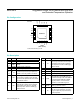
Figure 2. Human Body ESD Test Model Figure 3. Human Body Current Waveform
CHARGE-CURRENT-
LIMIT RESISTOR
DISCHARGE
RESISTANCE
STORAGE
CAPACITOR
C
S
100pF
HIGH-
VOLTAGE
DC
SOURCE
DEVICE
UNDER
TEST
100%
36.8%
t
RL
TIME
t
DL
PEAK-TO-PEAK RINGING
(NOT DRAWN TO SCALE)
I
r
0
0
I
PEAK
(AMPS)
90%
10%