
Datasheet


2 Maxim Integrated
40Mbps, +3.3V, RS-485 Half-Duplex
Transceivers
MAX14840E/MAX14841E
Stresses beyond those listed under “Absolute Maximum Ratings” may cause permanent damage to the device. These are stress ratings only, and functional
operation of the device at these or any other conditions beyond those indicated in the operational sections of the specifications is not implied. Exposure to absolute
maximum rating conditions for extended periods may affect device reliability.
(Voltages referenced to GND.)
V
CC
..................................................................... -0.3V to +6.0V
RE, RO
.................................................. -0.3V to +(V
CC
+ 0.3V)
DE, DI
.................................................................. -0.3V to +6.0V
A, B
.................................................................... -8.0V to +13.0V
Short-Circuit Duration (RO, A, B) to GND
............... Continuous
Continuous Power Dissipation (T
A
= +70NC)
8-Pin SO (derate 7.6mW/NC above +70NC)
............... 606mW
8-Pin TDFN (derate 24.4mW/NC above +70NC)
....... 1951mW
Junction-to-Case Thermal Resistance (B
JC
) (Note 1)
8-Pin SO
.......................................................................38NC/W
8-Pin TDFN
....................................................................8NC/W
Junction-to-Ambient Thermal Resistance (B
JA
) (Note 1)
8-Pin SO
.................................................................... 132NC/W
8-Pin TDFN
..................................................................41NC/W
Operating Temperature Range
...................... -40NC to +125NC
Junction Temperature
.................................................. +150NC
Storage Temperature Range
......................... -65NC to +150NC
Lead Temperature (soldering, 10s)
...............................+300NC
Soldering Temperature (reflow)
......................................+260NC
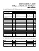
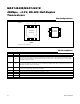
DC ELECTRICAL CHARACTERISTICS
(V
CC
= +3.0V to +3.6V, T
A
= -40NC to +125NC, unless otherwise noted. Typical values are at V
CC
= +3.3V and T
A
= +25NC.) (Notes 2, 3)
ABSOLUTE MAXIMUM RATINGS
Note 1: Package thermal resistances were obtained using the method described in JEDEC specification JESD51-7, using a four-layer
board. For detailed information on package thermal considerations, refer to www.maximintegrated.com/thermal-tutorial.
PARAMETER SYMBOL CONDITIONS MIN TYP MAX UNITS
POWER SUPPLY
Supply Voltage V
CC
3.0 3.6 V
Supply Current I
CC
DE = RE = V
CC
, or
DE = RE = GND, or
DE = V
CC
, RE = GND,
DI = V
CC
or GND, no load
1.5 4 mA
Shutdown Supply Current I
SH
DE = GND and RE = V
CC
10
FA
DRIVER
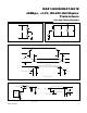
Differential Driver Output V
OD
R
L
= 54I, Figure 1
1.5 V
Change in Magnitude of
Differential Output Voltage
DV
OD
R
L
= 54I, Figure 1 (Note 4)
-0.2 0 +0.2 V
Driver Common-Mode Output
Voltage
V
OC
R
L
= 54I, Figure 1
V
CC
/2 3 V
Change in Common-Mode
Voltage
D
V
OC
R
L
= 54I, Figure 1 (Note 4)
-0.2 0.2 V
Single-Ended Driver Output High V
OH
A/B output, I
OUT
= -20mA 2.2 V
Single-Ended Driver Output Low V
OL
A/B output, I
OUT
= 20mA 0.8 V
Driver Short-Circuit Output
Current
|I
OSD
|
0V P V
OUT
P +12V, output low
250
mA
-7V P V
OUT
P V
CC
, output high
250
RECEIVER
Input Current (A and B) I
A,B
DE = GND,
V
CC
= GND or +3.6V
V
IN
= +12V 1000
FA
V
IN
= -7V -800
Differential Input Capacitance C
A,B
Between A and B, DE = GND, f = 2MHz 12 pF