
Datasheet


10 Maxim Integrated
40Mbps, +3.3V, RS-485 Half-Duplex
Transceivers
MAX14840E/MAX14841E
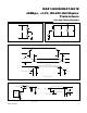
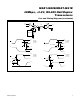
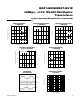
Pin Configurations
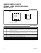
Pin Descriptions
A
GNDDI
1
2
8
7
V
CC
BRE
DE
RO
SO
3
4
6
5
MAX14840E
MAX14841E
1 3 4
8 6 5
V
CC
A GND
*EP
*CONNECT EXPOSED PAD (EP) TO GND.
MAX14840E
MAX14841E
2
7
B
RO
+
DE DIRE
TDFN
TOP VIEW
PIN NAME FUNCTION
1 RO Receiver Output. See the Function Table.
2
RE
Active-Low Receiver-Output Enable. Drive RE low to enable RO. RO is high impedance when RE is high.
Drive RE high and DE low to enter low-power shutdown mode. RE is a hot-swap input (see the Hot-Swap
Capability section for details).
3 DE
Driver-Output Enable. Drive DE high to enable driver outputs. These outputs are high impedance when
DE is low. Drive RE high and DE low to enter low-power shutdown mode. DE is a hot-swap input (see the
Hot-Swap Capability section for details).
4 DI
Driver Input. With DE high, a low on DI forces the A output low and the B output high. Similarly, a high on
DI forces the A output high and the B output low.
5 GND Ground
6 A Noninverting Receiver Input and Noninverting Driver Output
7 B Inverting Receiver Input and Inverting Driver Output
8 V
CC
Positive Supply Voltage Input. Bypass V
CC
with a 0.1FF ceramic capacitor to GND.
— EP Exposed Pad (TDFN Only). Connect EP to GND.