
Datasheet


MAX1444
10-Bit, 40Msps, 3.0V, Low-Power
ADC with Internal Reference
4 _______________________________________________________________________________________
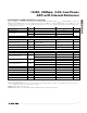
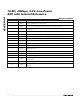
PARAMETER SYMBOL CONDITIONS MIN TYP MAX UNITS
Maximum REFP, COM Source
Current
I
S OU RC E
5mA
Maximum REFP, COM Sink
Current
I
SINK
-250 µA
Maximum REFN Source Current I
S OU RC E
250 µA
Maximum REFN Sink Current I
SINK
-5 mA
UNBUFFERED EXTERNAL REFERENCE (V
REFIN
= AGND, reference voltage applied to REFP, REFN, and COM)
REFP, REFN Input Resistance
R
REFP
,
R
REFN
Measured between REFP and COM
and REFN and COM
4kΩ
REFP, REFN, COM Input
Capacitance
C
IN
15 pF
Differential Reference Input
Voltage Range
ΔV
REF
ΔV
REF
= V
REFP
- V
REFN
1.024
±10%
V
COM Input Voltage Range V
COM
V
DD
/ 2
±10%
V
REFP Input Voltage V
REFP
V
C OM
+
ΔV
RE F
/
2
V
REFN Input Voltage V
REFN
V
COM
-
ΔV
REF
/
2
V
DIGITAL INPUTS (CLK, PD, OE)
CLK
0.8 ×
V
DD
Input High Threshold V
IH
PD, OE
0.8 ×
OV
DD
V
CLK
0.2 ×
V
DD
Input Low Threshold V
IL
PD, OE
0.2 ×
OV
DD
V
ELECTRICAL CHARACTERISTICS (continued)
(V
DD
= 3V; OV
DD
= 2.7V; 0.1µF and 1µF capacitors from REFP, REFN, and COM to GND; V
REFIN
= 2.048V; REFOUT connected to
REFIN through a 10kΩ resistor; V
IN
= 2V
P-P
(differential with respect to COM); C
L
= 10pF at digital outputs; f
CLK
= 40MHz; T
A
= T
MIN
to T
MAX
, unless otherwise noted. ≥ +25°C guaranteed by production test, < +25°C guaranteed by design and characterization; typi-
cal values are at T
A
= +25°C.)